Industry update — On 4 August 2026, NVM Express published its 2026 set of specifications, adding new security, manageability and quality-of-service features to the NVMe command set — the protocol keeps advancing while SATA stays fixed at its 6 Gb/s ceiling, sharpening the choice an FPGA designer makes between a SATA and an NVMe host core (NVM Express, 4 August 2026).
When you add solid-state storage to an FPGA, the first fork in the road is the interface: SATA vs NVMe. It is tempting to reach for NVMe simply because it is newer and faster — and with PCIe Gen5 SSDs and Gen5-capable FPGAs such as the Agilex 7 R-Tile now shipping in the current generation, the pull is stronger than ever. But that is the wrong way to decide. The right interface is set by your real sustained data rate, your logic budget and your latency needs. This comparison lays out the trade-offs plainly, using only public standard figures, so you choose the interface — and the IP core — that fits the job rather than the trend.
The short answer
Choose a SATA Host core when your sustained rate fits comfortably under a single SATA link (~600 MB/s) and you want the smallest, simplest design. Choose an NVMe Host core when you need multiple gigabytes per second, low latency, or modern M.2/U.2 drives. SATA wins on simplicity and logic cost; NVMe wins on raw performance. The decision is set by your data rate, not by which interface is newer.
Two interfaces, one job
Both SATA and NVMe let an FPGA read and write a solid-state drive, and both can be implemented as hardware IP cores with no soft CPU — a distinction worth understanding if you are new to licensing pre-verified logic (see our primer on what an FPGA IP core is, soft IP vs hard IP). The difference between the two is how they get the data across. SATA is a mature serial link designed in the hard-disk era and carried forward to SSDs; our SATA host and device IP selection guide covers that side in depth. NVMe was designed for flash from the start, running over PCIe with a deeply parallel command model — the subject of our complete guide to NVMe Host IP cores. That heritage explains every difference that follows.
Throughput: the headline difference
This is the main reason the choice exists, and the public standards make the gap concrete. A SATA III link is nominally 6 Gb/s, but 8b/10b line encoding and protocol overhead bring useful application throughput to roughly 600 MB/s — plenty for logging and many capture tasks, but a hard ceiling. NVMe runs over PCIe, where each generation roughly doubles the per-lane rate: a single PCIe Gen4 lane (16 GT/s, about 2 GB/s) already exceeds an entire SATA III link, a Gen4 x4 link clears several gigabytes per second, and PCIe Gen5 (32 GT/s per lane) doubles that again. If your stream needs that headroom, SATA simply cannot deliver it — and on a Gen5-capable device such as the Altera Agilex 7 R-Tile for Gen5 storage, an NVMe host core reaches the highest sustained write rates in the current FPGA generation.
Latency and parallelism
SATA uses a single command queue with limited depth. NVMe was built around many deep queues operating in parallel, which lowers latency and lets the drive stay busy. For a workload with lots of concurrent operations or strict latency targets — a high-speed data-acquisition recorder, for instance — NVMe’s queue model is a real advantage, but only if the host core actually keeps those queues fed. An NVMe core that under-feeds its queues behaves little better than SATA, for far more logic.
Logic footprint and complexity
SATA’s simpler protocol maps to a smaller, lighter core that fits comfortably even on modest FPGAs. NVMe’s queue management and PCIe handling cost more logic and memory, so it asks more of the device. On a small part, a full NVMe core can take a meaningful share of the fabric — or not fit alongside your application logic at all. That footprint difference is often the deciding factor on cost-optimized designs.
SATA vs NVMe side by side
| Criterion | SATA Host IP | NVMe Host IP |
|---|---|---|
| Physical link | SATA III, 6 Gb/s serial | PCIe Gen4 / Gen5, multiple lanes |
| Practical throughput | ~600 MB/s ceiling | Multiple GB/s (scales with lanes & generation) |
| Command model | Single queue, limited depth | Many deep parallel queues |
| Latency | Moderate | Lower |
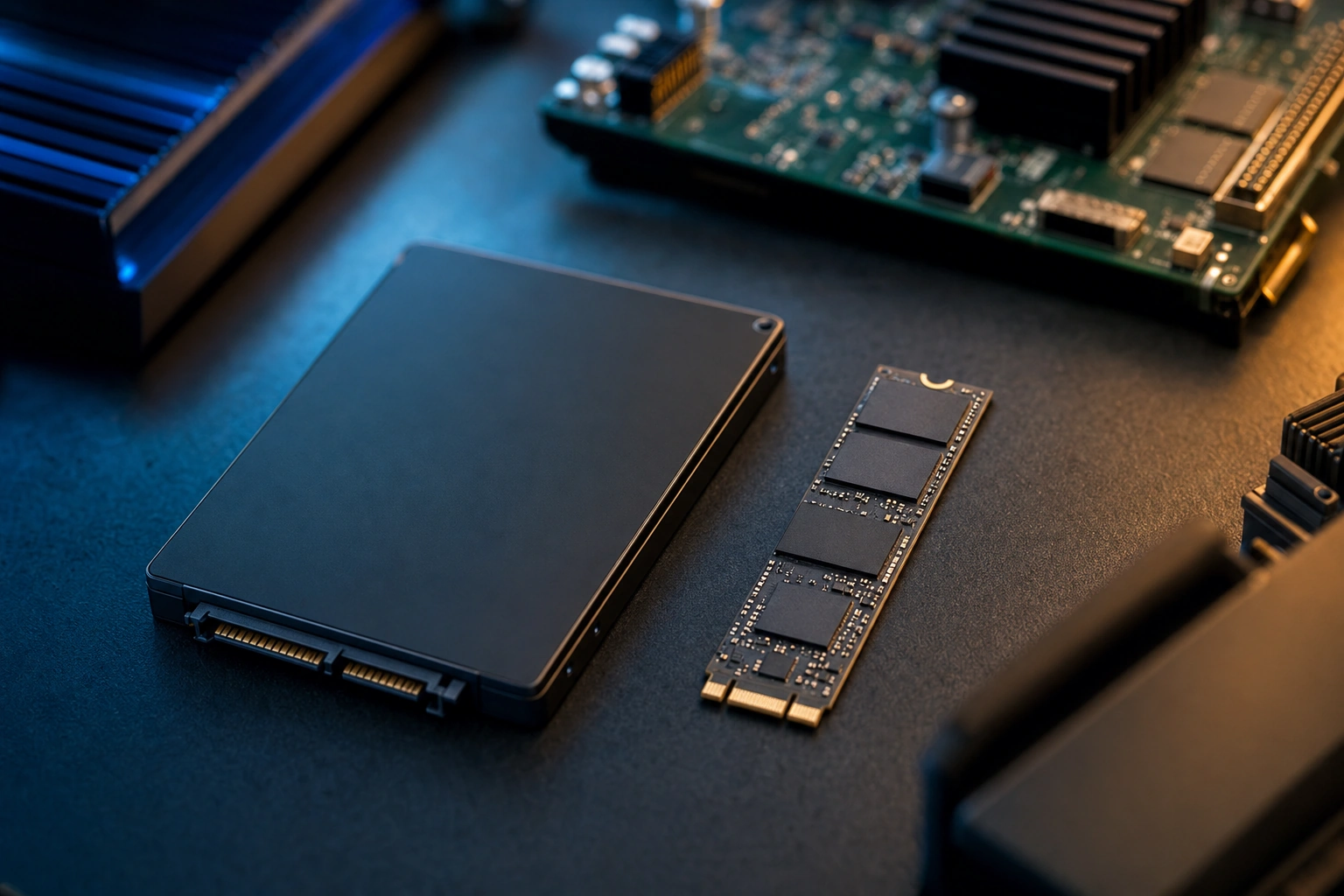
| Drive types | 2.5" SATA, mSATA | M.2 NVMe, U.2 |
| Logic footprint | Small | Moderate to large |
| CPU-less operation | Yes | Yes |
| Best for | Logging, telemetry, modest capture | High-rate recorders, video, radar |
Both cores run with no soft CPU and target AMD and Altera FPGAs. The real question is your sustained rate — let us help you pin it down.
How to decide
- Quantify your sustained rate. If it sits comfortably under ~600 MB/s, SATA is the efficient choice.
- Check latency needs. Strict latency or heavy concurrency favors NVMe’s queue model.
- Budget the logic. On a small FPGA, the lighter SATA core may be the only one that fits with your application.
- Look at the drives. If your form factor is M.2/U.2, NVMe is the natural match; 2.5" SATA SSDs point to SATA.
If the harder question is not which interface but which supplier, our buyer’s checklist for choosing an FPGA IP vendor walks through the questions that matter — support, portability and verification maturity.
Migrating from SATA to NVMe
Teams that started on SATA and now need more throughput can move to an NVMe host core, but it is a design change, not a drop-in swap: the link moves to PCIe, the logic budget grows, and the command model changes. Because a vendor that ships both the SATA and the NVMe host lines can keep the surrounding architecture consistent, the migration is far smoother than re-platforming across IP suppliers. Our NVMe Host IP guide details the target side of that move.
When neither is right
Sometimes a local SSD is the wrong answer entirely:
- Tiny data volumes. Configuration or calibration data belongs in QSPI flash or EEPROM, not on any SSD controller.
- Off-board destinations. If data must reach a server, an Ethernet or NVMe-over-Fabrics path beats a local drive.
- Extreme write endurance. For relentless write cycling, the SSD’s own endurance matters as much as the interface; the controller cannot save an under-specified drive.
Frequently asked questions
SATA vs NVMe for FPGA storage: which is better?
Neither is universally better. NVMe is faster but uses more logic. For modest data rates or small FPGAs, a SATA host core is smaller, simpler and cheaper. NVMe is worth its footprint only above the ~600 MB/s SATA throughput ceiling or when low latency matters.
How much faster is NVMe than SATA on an FPGA?
A SATA III link’s useful throughput is about 600 MB/s, while NVMe over PCIe reaches several gigabytes per second: a single Gen4 lane (~2 GB/s) already beats a whole SATA III link, and a Gen4 x4 or Gen5 link multiplies that further. The exact gap depends on PCIe generation, lane count and how well the NVMe queues are fed.
Do both SATA and NVMe cores work without a processor?
Yes. Both can be implemented as hardware IP cores that run entirely in FPGA logic, with no operating system and deterministic timing.
Which uses less FPGA logic, SATA or NVMe?
SATA. Its simpler protocol maps to a smaller core that fits even modest FPGAs. NVMe’s queue and PCIe handling cost more logic and memory.
Can I migrate a SATA design to NVMe later?
Yes, but it is a design change rather than a swap: the link moves to PCIe, the logic budget grows and the command model differs. Using a vendor that ships both cores keeps the surrounding architecture consistent.
Which interface should I pick for a high-rate recorder?
NVMe, in nearly all cases. Continuous high-rate recording — video, radar, dense sensor arrays — needs the multiple-gigabyte-per-second sustained throughput only NVMe delivers.
Still on the fence between SATA and NVMe for your design? Tell us your sustained data rate and target FPGA — the right answer usually falls out in minutes.