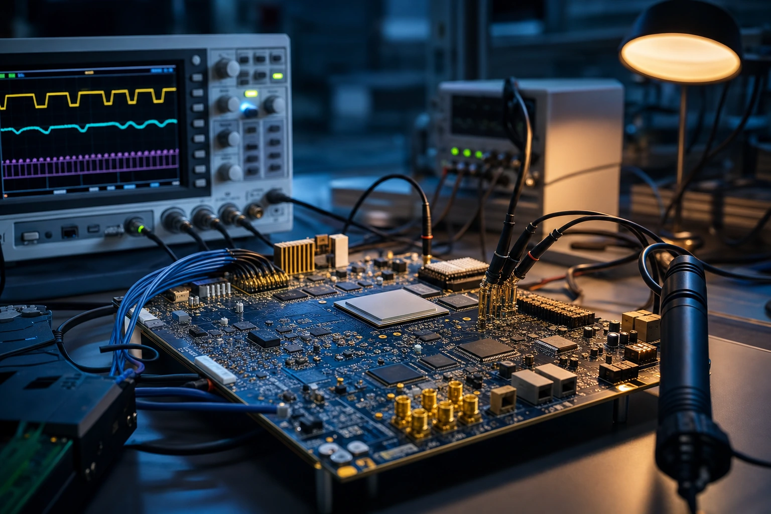
Industry update — On 8 June 2026, Altera introduced its Agilex 9 Direct RF-Series SoC FPGA with engineering samples and a claimed ~40% more compute per mm² — each new device family resets the timing, I/O and verification effort a team must absorb, which is exactly where an IP-focused FPGA design house earns its keep (Altera, 8 June 2026).
Updated 16 July 2026 · Written by the Logic Design Solutions engineering team · FPGA design house since 1994
Bottom line up front: FPGA design services from an IP-focused design house cover the full path from architecture to a validated bitstream — feasibility and device selection, RTL design, integration and customization of proven IP cores, and rigorous verification. What sets an IP-focused house apart from a generic RTL contractor is a head start from cores that are already proven, and verification depth that turns “it compiles” into “it is qualified”.
“FPGA design services” is a broad phrase that hides a lot of variation. A generic contractor writes the RTL you specify; an IP-focused design house brings something different to the table — a library of proven storage and data-bus cores, deep verification discipline, and the judgment to architect a system rather than just code a module. This guide explains what such a team actually delivers, where the value sits, and how it compresses a schedule that would otherwise run for months.
- The short answer
- What do FPGA design services cover?
- Architecture and device selection
- IP integration and customization
- Verification: the real differentiator
- Contractor vs IP-focused design house
- Custom FPGA development, end to end
- How does an engagement work?
- How to choose an FPGA design partner
- When services are not the right fit
- Frequently asked questions
The short answer
- Architecture & feasibility — device selection, interface mix and data-path sizing, before any RTL is written.
- RTL design — the custom logic, in the FPGA fabric of your chosen AMD or Altera family.
- IP integration & customization — dropping in proven cores (NVMe, SATA, ARINC 429, Ethernet) and adapting them at the source to your interfaces and constraints.
- Verification — proving the design behaves under corner cases and at sustained rate, with traceable evidence.
- Timing closure & delivery — meeting the clock, then handing over a build you can qualify.
The advantage over a generic RTL contractor is a head start from cores that are already proven, plus the verification depth regulated domains demand.
What do FPGA design services cover?
FPGA design services are the engineering work of turning a system requirement into a working, verified FPGA design — covering architecture and device selection, RTL, IP integration and customization, and verification, delivered as a bitstream you can put into a product. It helps to see the whole scope at once, because the value of a design house sits in the parts most teams underestimate — not the coding, but the architecture and the verification around it. A full FPGA design service spans five stages, and a good partner can enter at any one of them.
| Stage | What it delivers | Why it matters |
|---|---|---|
| Architecture & feasibility | Device, interfaces and data path chosen with margin | The most expensive mistakes are made here, before any RTL exists |
| RTL design | Custom logic in the FPGA fabric | The visible work — but rarely the risky part |
| IP integration & customization | Proven cores adapted to your system | Collapses months of protocol work into an integration task |
| Verification | Testbenches, sustained-rate checks, traceable evidence | Turns “it compiles” into “it is qualified” |
| Timing closure & delivery | A validated bitstream that meets the clock | A build you can trust and ship |
The stages you actually buy depend on where your own team is strong. Some clients want a turnkey custom FPGA development engagement from specification to bitstream; others already have the architecture and only need a storage interface integrated and verified. An IP-focused house can plug in at the layer where you need it.
Architecture and device selection: where the money is saved
The most expensive FPGA mistakes are made before a line of RTL exists. Pick a device that is too small and you discover it only after months of work. Underestimate the data path and your throughput target quietly becomes unreachable. A design house earns its fee here first: matching the FPGA family, the transceivers and the interface mix to what the system actually has to do, with margin built in.
For storage and high-speed data work, this means knowing which families carry the right PCIe tile or transceiver for the interface you need, and sizing the device for the IP cores plus your application logic. It also means settling questions that shape the whole design — such as SATA vs NVMe for a storage path — before they become costly to reverse. That judgment is hard to buy from a contractor who has not shipped the interface before.
IP integration and customization
This is where an IP-focused house pulls ahead. Instead of writing a SATA, NVMe, ARINC 429 or Ethernet controller from scratch, the team integrates a proven FPGA IP core it has already designed and verified, then customizes it to your interfaces, clocking and constraints. Months of protocol implementation and validation collapse into an integration task.
Customization matters because real systems are never the textbook case. The right buffering model for your throughput, the exact streaming interface to your fabric, a specific FPGA family port — these are adaptations a vendor who owns the source can make cleanly, where a black-box licensee cannot. That is the practical benefit of IP reuse: you inherit a mature core and still get it fitted to your design.
The cores that anchor an integration
For storage and data-bus work, the reusable pieces are usually the hardest parts of the design to get right:
- Storage — NVMe Host IP for high-bandwidth PCIe SSD paths, and SATA host and device IP for cost-sensitive or legacy interfaces.
- Data bus — ARINC 429 data-bus IP for avionics and instrumentation.
- Connectivity — Ethernet cores for streaming and control planes.
Verification: the real differentiator
Anyone can make RTL compile. Proving it behaves correctly — across corner cases, error conditions and sustained rate — is the work that separates a demo from a product. For storage and data-bus IP, verification is the larger share of the effort, and it is exactly what teams under schedule pressure are tempted to cut.
A disciplined design house treats verification as a first-class deliverable: testbenches that exercise the protocol, sustained-rate checks at the bench with real instruments, and traceable evidence that each function does what the specification says. In avionics, defense and instrumentation — where an ARINC 429 interface may sit inside a certified system — that traceability is not optional. It is the basis of qualification.
Weighing whether to build a storage or data-bus controller in-house or license a proven core and have it integrated? A short scoping call usually clarifies the trade-off.
Contractor vs IP-focused design house: what is the difference?
A generic FPGA contractor sells hours of RTL coding. An IP-focused design house sells outcomes built on assets it already owns. The difference shows up across the whole engagement.
| Dimension | Generic RTL contractor | IP-focused design house |
|---|---|---|
| Starting point | Writes each block from your spec | Integrates cores already designed and verified |
| Hard interfaces | Implemented from scratch, schedule risk | Reused and customized at the source |
| Verification | Often scoped to time available | First-class deliverable, traceable |
| Customization | Limited by black-box licensed IP | Full, because it owns the source |
| Schedule on storage/bus work | Longer — protocol built from zero | Shorter — integration, not implementation |
When the hard part of your design is a storage or data-bus interface, that distinction is the whole game: shorter schedules, lower risk on the difficult interfaces, and the ability to customize at the source rather than work around a closed core.
Custom FPGA development, end to end
Some projects need more than an integrated core — they need a system built. A full custom FPGA development engagement runs from a written specification through architecture, RTL, integration, verification and timing closure to a delivered, validated bitstream. The proven-IP library still helps here: the storage and bus pieces are reused, so the bespoke effort concentrates on what is genuinely unique to your application — a custom capture pipeline, a specialized control plane, or a high-speed data-acquisition recorder that has to keep pace with its sensor stream without dropping data.
How does an engagement work?
A typical FPGA design engagement moves through five steps. The first two settle most of the risk before significant effort is committed.
- Scope & feasibility — you describe the system; the team assesses the device, interfaces and data path, and confirms the target is reachable.
- Architecture — the data path, IP selection and device are fixed, with throughput margin designed in.
- Integration & design — proven cores are integrated and customized; bespoke logic is written around them.
- Verification & closure — the design is proven against the specification and meets timing.
- Delivery — a validated bitstream, with the verification evidence to back it.
How to choose an FPGA design partner
Not every FPGA team is the right fit for every project. When the difficult part of your design is a storage or data-bus interface, weight your choice toward a partner that owns proven IP in that domain rather than one that would build it from scratch. A few questions separate them quickly: Does the partner own and maintain the core, or license it as a black box? Can they show verification evidence, not just a compiling design? Do they support both AMD and Altera families, so the device decision is made on system merits? Our FPGA IP vendor buyer’s checklist works through the full list; the short version is that source ownership and verification discipline matter more than headcount.
When services are not the right fit
Design services are not always the answer:
- You only need the core. If your team can integrate and verify, licensing the IP core alone is more economical than a full engagement.
- The work is pure firmware or software. An FPGA design house focuses on logic and interfaces, not application software stacks.
- The interface is fully standard and you have done it before. If your in-house team already ships the interface reliably, external help adds less.
Frequently asked questions
What do FPGA design services include?
Architecture and feasibility, device selection, RTL design, integration and customization of proven IP cores, verification, timing closure and delivery of a validated bitstream — the full path from specification to a build you can qualify. A good partner can enter at any stage rather than only turnkey.
How is an IP-focused design house different from a contractor?
A contractor writes the RTL you specify, by the hour. An IP-focused house integrates cores it already designed and verified, customizes them at the source, and applies deeper verification — shortening schedules and reducing risk on hard interfaces such as NVMe, SATA and ARINC 429.
Can I license just the IP core instead of a full design service?
Yes. If your team can integrate and verify, licensing the core alone is the economical path. The full design service is for projects that also need architecture, integration or verification help.
Do FPGA design services cover both AMD and Altera FPGAs?
Yes. Cores such as NVMe, SATA, ARINC 429 and Ethernet target AMD (Xilinx) and Altera families, so the device decision can be made on system merits rather than being forced by IP availability.
Why is verification emphasized so much in FPGA design?
Because making RTL compile is easy; proving it behaves under corner cases and at sustained rate is the hard, schedule-determining work. For avionics, defense and instrumentation, traceable verification is the basis of qualification.
What deliverable do I get at the end of a custom FPGA development project?
A validated bitstream meeting your timing and throughput targets, together with the verification evidence behind it — not just code that compiles.
How long does an FPGA design engagement take?
It depends on scope, but reusing proven IP for the hard interfaces is the biggest lever on schedule: it collapses months of protocol implementation and validation into an integration task, so the bespoke effort concentrates on what is unique to your application. A scoping call is the fastest way to get a realistic estimate for your project.
Have an FPGA project that needs architecture, integration or verification help — or a storage interface you would rather license than build? Tell us the scope.