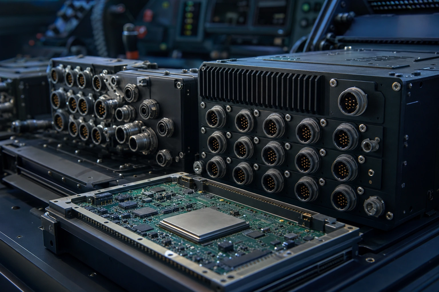
Industry update — On 25 March 2026, Frontgrade Gaisler announced its GR740 processor was selected for ESA’s RAMSES mission and unveiled a Versal-powered SpaceVPX platform — confirming that avionics and space systems keep pushing deterministic data buses like ARINC 429 onto FPGAs, where reliability and certification evidence matter most (Frontgrade Gaisler, 25 March 2026).
ARINC 429 is the quiet workhorse of commercial avionics: a simple, robust, one-way serial data bus that has carried flight data between aircraft systems since the late 1970s and still ships on new airframes today. Implementing the ARINC 429 protocol in an FPGA with a dedicated ARINC 429 IP core gives you deterministic, hardware-level transmit and receive channels — no soft processor, no software stack to certify. This guide explains the protocol in plain terms, walks through the 32-bit word bit by bit, shows what the core actually handles on transmit and receive, and explains why a hardware implementation is the natural fit for certifiable systems.
The short answer
An ARINC 429 IP core implements the avionics data bus directly in FPGA logic, providing transmit and receive channels that handle the 32-bit word format, label decoding, parity and the two standard bit rates — all without a soft processor. Because the protocol lives in hardware, the timing is deterministic and each function maps cleanly to a requirement, which is exactly what avionics qualification demands.
What ARINC 429 is
ARINC 429 is a unidirectional serial data bus defined by the Airlines Electronic Engineering Committee (AEEC) and published through SAE ITC. It is used across commercial aircraft to move parameters — altitude, airspeed, heading, system status — between line-replaceable units. Each bus has exactly one transmitter and up to twenty receivers; data flows one way only. That constraint is the point: a one-way, well-defined bus is easy to reason about and hard to get subtly wrong, which is why the ARINC 429 protocol has endured for more than four decades.
A system that needs to both send and receive ARINC 429 simply uses separate transmit and receive channels. An FPGA is an ideal home for this, because it can host many independent channels in parallel, each running deterministically. If the term “IP core” is new to you, it helps to first understand what an FPGA IP core is and how soft IP differs from hard IP before mapping the protocol onto silicon.
The 32-bit word: labels, data, parity
Everything on ARINC 429 travels as a fixed 32-bit word, and every word uses the same field layout. That consistency is what makes a hardware decoder clean to build and easy to verify. The bits are numbered 1 through 32, and each range has a defined role:
| Bits | Field | Role |
|---|---|---|
| 1–8 | Label | Identifies the type of data the word carries (the parameter). Transmitted first, and conventionally expressed in octal. |
| 9–10 | SDI | Source/Destination Identifier — distinguishes among multiple sources or sinks sharing a label. |
| 11–29 | Data | The 19-bit payload, encoded as BNR (binary), BCD (decimal) or discrete bits depending on the parameter. |
| 30–31 | SSM | Sign/Status Matrix — conveys sign, or the validity and operational status of the data. |
| 32 | Parity | A single parity bit, typically odd, for per-word error detection. |
The label is the heart of it: a receiver filters the bus by label to pick out only the parameters it cares about. A good IP core exposes that label-based handling directly, so your application logic deals in meaningful parameters rather than raw bits.
Speeds, encoding and channels
ARINC 429 runs at two standard bit rates: a high speed of 100 kbit/s and a low speed in the 12–14.5 kbit/s range. There is no separate clock line — the bus self-clocks using bipolar return-to-zero (RZ) encoding, a tri-level scheme of HI, NULL and LO voltage states, with a gap of at least four bit-times between words to mark word boundaries. An FPGA core recovers this timing for both rates in hardware. Because each channel is independent logic, a single FPGA can serve a whole avionics box with many transmit and receive lines at once — a density that is hard to match with discrete transceivers.
Transmit and receive: what each side does
The two directions are separate hardware paths, and it is worth being precise about what each one is responsible for, because that division is exactly what an IP core encapsulates.
On the receive side, the channel recovers bit timing from the self-clocked line, assembles each 32-bit word, verifies the parity bit, optionally checks the SDI, and filters by label — often against a programmable label table — so downstream logic only ever sees the parameters it asked for. Received words are usually buffered in a FIFO so bursts do not stall the application.
On the transmit side, the channel takes a parameter and label from your logic, assembles the 32-bit word, computes the parity bit, and drives the line at the selected rate with correct RZ encoding and inter-word gaps. Both directions run without any processor in the loop, which is what keeps the timing deterministic.
What the IP core handles
A dedicated ARINC 429 core takes all of that protocol detail off your plate. It presents a clean parameter-and-label interface to your application and absorbs the bit-level work — timing recovery, word framing, parity, label filtering and line encoding — inside the fabric. Your logic deals in parameters and labels; the core deals in bits and timing. If you are weighing a licensed core against building your own, the trade-offs are the same ones covered in this buyer’s checklist for choosing an FPGA IP vendor.
Avionics designs often combine ARINC 429 with high-speed recording. Need both a data bus and a storage path in one FPGA? Let us scope it.
Why a hardware core suits avionics
Avionics qualification rewards determinism and traceability. A software ARINC stack running on a processor introduces scheduling variability and a body of code that must itself be verified. A hardware core in the FPGA fabric has neither problem: the timing is fixed by the logic, the behavior is repeatable word for word, and each function maps cleanly to a requirement. Airborne electronic hardware is commonly developed under design-assurance frameworks such as RTCA/DO-254, and that requirement-to-logic traceability is precisely what such processes look for. (Design assurance is a property of a full project and its evidence, not of an IP block in isolation — a well-structured core supports the effort but does not replace it.)
The determinism argument is the same one that governs the wider build-versus-buy and hardware-versus-software question in FPGA design; if that trade-off is what you are really weighing, this piece on FPGA versus ASIC and why IP reuse matters lays out the reasoning. A hardware core also pairs naturally with the rest of an avionics mission system: data captured off ARINC 429 can flow straight into a hardware storage path on the same device, with no processor in the loop — the pattern behind an NVMe host recorder IP for high-speed data acquisition.
FPGA family support
Because ARINC 429 is a low-rate, robust protocol, a core fits comfortably on a wide range of FPGA families, including cost-optimized parts from AMD (Xilinx) and Altera. The deciding factors are usually the channel count you need and the surrounding interfaces in your design, not the raw capability of the device. The core can sit alongside storage and connectivity IP on the same FPGA, which is common in avionics data-acquisition and recorder designs — where a bus interface is often integrated with an NVMe host IP core for FPGA storage or a SATA host and device IP path. Delivering that kind of integrated, IP-focused design is the core of what an IP-focused FPGA design house delivers.
Where ARINC 429 stops
ARINC 429 is the right bus for a large class of avionics signals, but not all of them:
- High-bandwidth payloads. At up to 100 kbit/s, ARINC 429 is for parameters and status, not video or bulk data — those belong on a high-speed bus or a storage path.
- Bidirectional, high-determinism networks. Where systems need command/response or fault tolerance beyond a one-way bus, MIL-STD-1553 or newer avionics networks fit better.
- Modern high-rate avionics data buses. ARINC 664 / AFDX addresses switched, high-bandwidth avionics networking; ARINC 429 remains the simple, reliable parameter bus alongside it.
Frequently asked questions
What is an ARINC 429 IP core?
A block of FPGA logic that implements the ARINC 429 avionics data bus — transmit and receive channels handling the 32-bit word format, label filtering, parity and the standard bit rates — entirely in hardware, with no soft processor.
How many bits is an ARINC 429 word?
Every ARINC 429 word is 32 bits: an 8-bit label (bits 1–8), a 2-bit SDI (bits 9–10), a 19-bit data field (bits 11–29), a 2-bit Sign/Status Matrix (bits 30–31) and a parity bit (bit 32). The label identifies which parameter the word carries.
What bit rates does the ARINC 429 protocol use?
Two standard rates: a high speed of 100 kbit/s and a low speed in the 12–14.5 kbit/s range. The bus self-clocks with bipolar return-to-zero encoding and a gap of at least four bit-times between words.
Why implement ARINC 429 in an FPGA instead of software?
A hardware core gives deterministic timing and repeatable, traceable behavior with no operating system or driver to verify — the properties avionics qualification rewards. It also hosts many independent channels in parallel.
Can one FPGA handle many ARINC 429 channels?
Yes. Each channel is independent logic, so a single FPGA can serve a whole avionics box with many transmit and receive lines simultaneously, each running deterministically.
How does ARINC 429 compare with MIL-STD-1553?
ARINC 429 is a simple one-way parameter bus; MIL-STD-1553 is a bidirectional, command/response military data bus with higher determinism and fault-tolerance features. They suit different roles in avionics systems.
Building an avionics system that needs ARINC 429 transmit and receive channels in FPGA hardware? Tell us your channel count and target family.