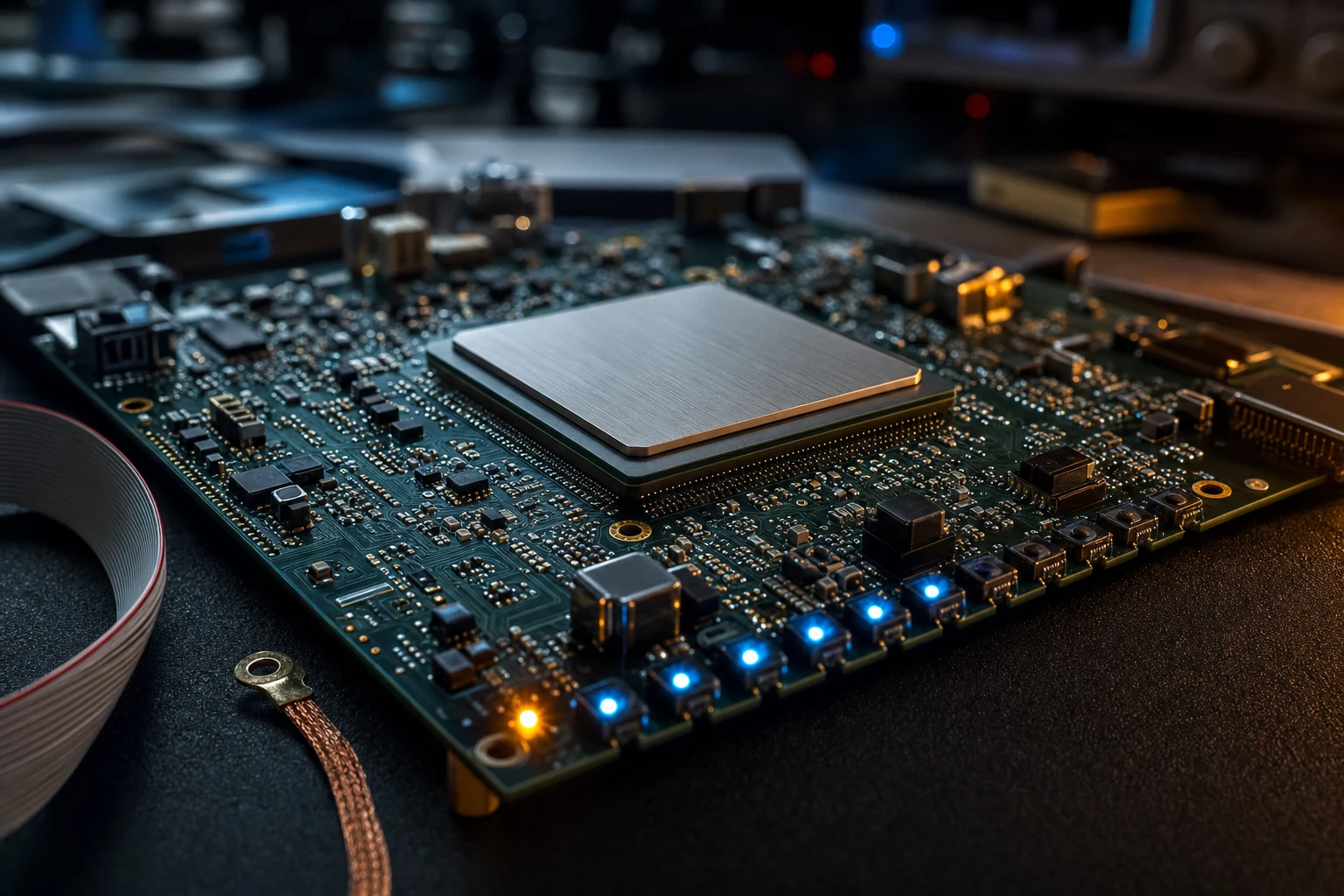
Industry news — On 2 September 2026 QuickLogic unveiled a next-generation embedded FPGA hard IP for GlobalFoundries’ 12LP process, able to scale beyond 250,000 look-up tables and offering an optional configuration bit health monitor that detects and corrects single-event-upset errors while the user design is still running — a sign that the FPGA is no longer only a chip you buy, but increasingly a block designers drop inside their own silicon (QuickLogic, 2 September 2026).
In short: An FPGA is an integrated circuit whose logic function is defined after manufacture by a configuration bitstream — a fabric of look-up tables and flip-flops, surrounded by block RAM, DSP slices, clock managers, I/O banks and serial transceivers, with a few functions such as PCI Express hardened into silicon.
Two hundred and fifty thousand look-up tables. That is the unit an FPGA vendor reaches for when it wants to tell you how big a fabric is, in the same way a processor vendor reaches for cores and a memory vendor reaches for gigabytes. So the first question a system designer should ask is the obvious one: what is a look-up table, why is it the currency of this technology rather than the gate or the transistor, and what else is in the chip around it? This article answers that from the architect’s chair rather than the lecture theatre. It assumes you know what an integrated circuit is and what a register does, and it aims to leave you able to read an FPGA datasheet, size a design, hold a credible conversation with a vendor, and — the part most primers skip — recognise the cases where the answer to your problem is not an FPGA at all.
- The short answer
- What an FPGA is, and how it differs from an ASIC
- The fabric, block by block
- Hard blocks versus soft logic
- Configuration technology, and what it implies
- The design flow, honestly
- The three vendors and their FPGA families
- When an FPGA is the right answer, and when it is not
- Where licensed IP comes in
- Where this stops applying
- Frequently asked questions
The short answer
A field-programmable gate array is an integrated circuit whose logic
function is defined after manufacture, by loading a configuration bitstream that
sets the contents of thousands of small memories and the state of the switches wiring them together.
The silicon leaves the factory generic; your design makes it specific, and a different bitstream
makes it something else. The fabric is a regular array of look-up tables and flip-flops surrounded by
dedicated resources — block RAM, DSP slices, carry chains, clock managers, configurable I/O
banks and serial transceivers — plus hardened blocks such as a PCI Express controller, a memory
controller or, on SoC devices, a full processor complex. Everything you write in VHDL or Verilog that
is not one of those hard blocks becomes look-up tables and flip-flops. That sentence governs most of
what follows.
What an FPGA is, and how it differs from an ASIC
An FPGA is programmable in a sense that has nothing to do with software. You are not writing
instructions a processor fetches and executes; you are describing a circuit, and the tools build that
circuit out of the configurable resources on the die. When the design runs there is no program
counter and no instruction stream — only a network of logic and registers, clocked, all of it
operating at once. That is what makes FPGAs good at line-rate work, and what makes them unfamiliar to
anyone arriving from software.
The contrast people reach for is the application-specific integrated circuit: a chip
whose transistors are committed at fabrication. An ASIC beats an equivalent FPGA design on unit cost
at volume, on power and on achievable clock frequency, because nothing on the die is spent being
flexible. What it costs is a mask set, a long development cycle, and a bug found after tape-out that
is a new mask set rather than a new bitstream. An FPGA pays a permanent overhead in area, power and
frequency in exchange for a correction that takes an afternoon. That trade — including what IP
reuse does to the economics — is argued properly in
FPGA versus ASIC and why IP
reuse matters. The rest of this article assumes you have landed on an FPGA and want to know what
is inside one.
The fabric, block by block
The fabric is a two-dimensional array of identical logic tiles embedded in a sea of programmable
interconnect, with columns of specialised resources cutting through it. Vendors use different names
for the same ideas, which is the main obstacle to reading two datasheets side by side.
Look-up tables, flip-flops and the logic tile
A look-up table is a small memory holding the truth table of a Boolean function. Give a
six-input LUT the sixty-four output values of the function you want and it produces the right answer
for any input combination in one propagation delay, with no notion of what the function means.
AMD’s UltraScale Architecture Configurable Logic Block User Guide documents a
six-input LUT that can alternatively be used as two five-input LUTs with shared inputs. That is why
LUT count is the currency of this technology: it is the only unit that maps directly onto arbitrary
combinational logic.
A flip-flop stores one bit and updates it on a clock edge. LUTs compute, flip-flops
remember, and essentially every synchronous design is those two wired together. Vendors group them
into a tile — AMD calls it a slice inside a configurable logic block, Altera calls its unit an
adaptive logic module, Microchip calls its unit a logic element. The grouping matters because
elements inside one tile share fast dedicated paths, and anything crossing between tiles pays for
general routing.
Distributed RAM, block RAM, DSP slices and carry chains
The same LUTs can be repurposed as memory. Distributed RAM uses the LUT storage cells
as a small, shallow RAM — AMD documents it as a SLICEM-only capability with synchronous write
and asynchronous read — and it is the right structure for a sixteen-entry buffer or a short
delay line. Block RAM is the opposite: hardened dual-port SRAM in columns through the
fabric, in fixed sizes that can be split or cascaded, with built-in FIFO controllers and, on many
families, error-correcting code. Larger devices add a deeper hardened memory tier again. Distributed
RAM costs you logic, block RAM does not, and running out of block RAM is a common way a design stops
fitting.
A DSP slice is a hardened arithmetic block — typically a pre-adder, a multiplier
and an accumulator with pipeline registers — because building a wide multiplier from LUTs is
possible, expensive and slow. Filters, transforms and control loops land here, and DSP column count
is a real constraint on signal-processing designs. The carry chain is narrower but as
important: a fast dedicated path propagating a carry vertically through adjacent tiles, so a wide
adder or comparator does not have to ripple through general routing.
Routing and switch matrices
The routing fabric is the majority of the die area, and it is where designs actually
fail. Each logic tile connects to a switch matrix, a programmable crossbar steering
signals onto wire segments of varying length. A net between two distant tiles is a chain of segments
and switches, and every switch adds delay. The consequence is architectural rather than academic: a
design only sixty per cent full can still fail timing because the tools could not find a short enough
path, which is why locality is a design skill and not a tooling detail.
I/O banks, clock regions, PLLs and transceivers
Pins are grouped into I/O banks, and each bank has its own supply voltage. That
constrains which single-ended and differential I/O standards the pins in that bank can use, and two
peripherals at different voltages cannot share a bank — which is why bank allocation belongs in
the schematic review rather than in bring-up.
Clocking is equally structured. The fabric is divided into clock regions, each served by
dedicated low-skew networks, so a clock spread across every region costs more clocking resource than
one kept local. Feeding those networks are the mixed-mode clock managers and phase-locked
loops that synthesise the frequencies a design needs from the few oscillators on the board, remove
insertion delay and shift phase — the blocks AMD documents in its UltraScale clocking
guide.
The serial transceiver, or SerDes, is what makes an FPGA useful at multi-gigabit rates.
It is hardened analogue and mixed-signal silicon: a serialiser and deserialiser, a clock-data
recovery loop, transmit pre-emphasis and receive equalisation, and encoding such as 8b/10b or 64b/66b.
It carries PCI Express, SATA at 1.5 Gbps, 3 Gbps and 6 Gbps, and 10 Gbps Ethernet
off the device. You cannot build one out of LUTs, and transceiver count and grade is frequently the
reason a particular part is chosen.
Hard blocks versus soft logic
Some functions are fixed silicon and the rest is fabric, and knowing which is which is the most
useful thing you can bring to a scoping meeting. A hard block is a dedicated circuit on
the die that you enable and configure rather than build: the PCI Express controller, the DDR memory
controller, the Ethernet MAC on some families, the analogue system monitor, and on SoC-class devices
an entire processor complex — Arm application and real-time cores on AMD Zynq and Zynq
UltraScale+ parts, a RISC-V complex on Microchip PolarFire SoC.
Hard blocks are free in fabric terms and fixed in behaviour. They consume no LUTs, they run faster
than anything you could assemble, and they come characterised. What you give up is flexibility: a
hard PCIe controller supports the lane counts, generations and modes its designers chose, and
anything outside that envelope puts you back in the fabric. The other half of the rule is unforgiving
in the opposite direction — every protocol engine, state machine, filter and bus fabric you
write becomes look-up tables and flip-flops, competing for the same finite supply. That is why
“we will just add a second channel” deserves a resource estimate before anyone agrees to
it.
PCI Express is the clearest case of the boundary, because it is almost always a hard block whose
transaction layer you still have to drive with your own logic; how that division works, and where
root complex and endpoint roles land, is covered in
PCIe on FPGA. The general
distinction between silicon you enable and logic you license or write belongs to
what an FPGA IP core is, soft IP versus
hard IP; the one-line version is that hard IP is fixed and free but unportable, and soft IP costs
fabric and buys you portability and visibility.
Configuration technology, and what it implies
Two configuration technologies are in production, and the difference between them is one of the
few genuinely architectural choices that a datasheet comparison will not make for you.
In an SRAM-based FPGA — the AMD and Altera families, and the great majority of
devices in the field — the configuration memory is volatile. At every power-up the bitstream
must be loaded, either by the device fetching it from an external non-volatile memory or by a host
pushing it in; AMD’s UltraScale Architecture Configuration User Guide documents master
SPI and master BPI modes reading from external flash alongside the JTAG and SelectMAP paths. Two
consequences follow. The configuration flash is part of your bill of materials and your boot-time
budget, and nothing runs until that load completes. And the configuration cells are memory cells, so
a passing particle can flip one — a single-event upset. A corrupted configuration
bit does not crash a program; it silently changes the circuit. AMD ships a dedicated mitigation core
for exactly this, described in its product guide as a solution “to detect and correct soft
errors in Configuration Memory of AMD FPGAs”, and it is the same problem the QuickLogic
announcement above addresses with a configuration bit health monitor.
In a flash-based FPGA — Microchip’s IGLOO2, SmartFusion2, PolarFire,
PolarFire SoC and the radiation-tolerant RTG4 — the configuration lives in non-volatile flash
cells on the die itself. The device is live at power-up with no external configuration memory and no
load sequence, which removes a component, a boot delay and a window during which the system is
undefined. And because a flash cell is not an SRAM cell, the configuration is not susceptible to
single-event upset the way an SRAM fabric is. That immunity is specifically about the configuration:
the flip-flops and block RAM holding your design’s state are ordinary memory and still
need mitigation if the environment demands it. For space, high-altitude avionics and long unattended
deployments that distinction drives the device choice, and we treat it properly in
radiation-hardened and
space-grade FPGAs.
The design flow, honestly
The FPGA design flow is a sequence of transformations from intent to a bitstream, and each stage
can reject the work of the one before it:
- Specification. Interfaces, rates, latency budgets, clock domains and the target
device. Choosing the device late is a common and expensive error: transceiver count, I/O bank
voltages and hard-block availability constrain the architecture. - RTL. The design described at register-transfer level in VHDL or Verilog —
or generated from C or C++ by a high-level synthesis tool, which shifts effort rather than removing
it. - Simulation. Functional verification against a testbench, before any hardware
exists. Most bugs are found here, and on a serious design most of the schedule goes here. - Synthesis. The RTL mapped onto device primitives: LUTs, flip-flops, block RAM,
DSP slices, carry chains. - Place and route. Every primitive assigned a physical location, and every net a
physical path through the switch matrices. - Static timing analysis. The delay of every path computed against your declared
clock constraints, and a verdict on whether the design meets timing. - Bitstream generation and bring-up. The configuration file is produced and
loaded, and the design meets the real world.
Place and route is not a compile, and treating it as one is the most common planning
mistake newcomers make. It is a large combinatorial optimisation over a congested physical device,
and on a full design in a big part a single implementation run is measured in hours rather than
seconds. You do not iterate on it the way you iterate on software. The corollary is that
timing closure is a distinct engineering activity with its own techniques, and it is where
high-speed interface projects tend to lose their schedule — the subject of our note on
timing closure on high-speed
storage interfaces.
Then there is bring-up, which no simulation replaces. The instrument is the embedded logic
analyser: a block instantiated in your own fabric that captures internal signals into block RAM
on a trigger condition and streams them out over JTAG. AMD calls its version the Integrated Logic
Analyzer, Altera provides Signal Tap, Microchip provides SmartDebug. It costs you resources and it
requires another implementation run to change what you are watching — which is precisely why
place-and-route runtime matters. The whole path from a written specification to a validated bitstream
is set out in custom FPGA
development from spec to validated bitstream.
The three vendors and their FPGA families
Three vendors are worth knowing at the architectural level, and each one segments its catalogue
the same way — a cost-optimised line, a mid-range line and a high-end line — with SoC and
specialist parts alongside. Note that Altera has been an independent company since
2024; Cyclone, Arria, Stratix and Agilex are Altera devices.
| Vendor | Cost-optimised | Mid-range | High-end | SoC and specialist | Distinguishing characteristic |
|---|---|---|---|---|---|
| AMD (former Xilinx lines) |
Spartan, Artix | Kintex | Virtex | Zynq and Zynq UltraScale+ (Arm cores), Versal adaptive SoC | The broadest catalogue and the largest third-party ecosystem; UltraScale and UltraScale+ are architecture generations spanning the tiers. |
| Altera (independent since 2024) |
Cyclone | Arria | Stratix | Agilex, segmented from Agilex 3 through Agilex 9 | Agilex is the current generation across tiers, with strong transceiver and high-bandwidth-memory positioning at the top of the range. |
| Microchip | IGLOO2 | PolarFire | PolarFire, top densities | SmartFusion2 (Arm Cortex-M3), PolarFire SoC (RISC-V), RTG4 for space | Flash-based fabric: live at power-up, no external configuration memory, and configuration immune to single-event upset. |
Two things follow from that table. Tier names are not comparable across vendors — only
transceiver count, logic capacity, hard-block list and I/O will tell you whether two parts are
equivalent. And Microchip is a different kind of choice rather than a cheaper version of the same
one: the flash fabric, and the low static power that comes with it, is the reason to be there. Which
family suits a storage design in particular is the subject of
choosing an FPGA for storage
IP.
When an FPGA is the right answer, and when it is not
An FPGA is the right answer when the problem has a shape that fixed hardware fits and general
processors do not:
- Sustained line-rate processing. Data arrives continuously at a rate that must
never be missed — a sensor stream, a radar front end, a recorder writing to SSD — and one
sample per clock is the natural structure. - Low, bounded latency. Not average latency: worst-case, guaranteed, with no
scheduler and no cache in the path. - Wide, custom or legacy I/O. A protocol no standard part implements, an obsolete
interface that still has to be supported, or simply more parallel pins than a controller
offers. - Fine-grained parallelism. Hundreds of identical small operations running at once
rather than a few large ones. - Long lifetimes and field updates. Twenty-year avionics, industrial and defence
programmes where the logic must stay correctable in the field.
It is the wrong answer at least as often, and saying so is what separates a design partner from a
salesperson. Control-flow-heavy software — parsing, decision trees, protocol state that changes
shape every quarter — belongs on a processor, as our comparison of
FPGA versus CPU sets out. If a
microcontroller already carries the peripherals you need, an FPGA is a large step in cost, power,
board complexity and engineering time, and
FPGA versus microcontroller for
high-throughput I/O draws the line where throughput and determinism justify the move. Very high
volume with a stable design is the ASIC case. And if nobody on the team writes RTL, high-level
synthesis narrows the gap but does not close it: timing closure, clock-domain crossing and bring-up
remain hardware skills, and a first project without them takes longer than anyone plans for.
Where licensed IP comes in
Most of a real FPGA design is not written by the team that ships it. The differentiating logic
— the algorithm, the control law, the thing the product exists for — is usually a
minority of the fabric. The majority is infrastructure: a storage controller, a bus interface, a
network MAC, a serial peripheral, a file system. Each of those is a standard somebody has already
implemented and, more to the point, already verified against real hardware that does not behave the
way the specification says it should.
That is the market a soft-IP vendor serves. As a factual example, Logic Design Solutions publishes
a catalogue of FPGA IP cores covering SATA host and device controllers, NVMe host controllers
including recorder variants, a 10 Gbps Ethernet MAC described on its product page as
“compliant with IEEE802.3ae specification”, ARINC 429 transmit and receive
controllers supporting all ARINC 429 data rates and up to 2.5 Mbit/s, and the small serial
macros every board needs — I2C master and slave, SPI master and slave, and UART. The published
feature lists are specific in the way an engineer can check: the I2C master is stated as compliant
with the I2C-bus specification with a system clock up to 180 MHz, the SPI slave up to
220 MHz, and the NVMe host line is published with 512 B and 4096 B sector support.
Delivery is in source — the product pages state the cores are “Available in VHDL source
code format for ease of customization”, and for the avionics-facing cores that
“DO254 design, verification and traceability documentation available on request”.
Whether you license or build, the reasoning is the one that runs through this whole article.
Fabric is finite, hard blocks are fixed, place and route is slow, and verification is where the
schedule really goes. Spending your team’s time on the block that makes your product
different, and licensing the blocks that merely have to be correct, is not a procurement preference
— it is the same resource-allocation logic that decides everything else in an FPGA design.
Tell us the interface you have to support, the rate it has to run at and the device you are considering, and we will tell you what that costs in fabric, what is already hardened on that part, and what is worth licensing rather than writing.
Where this stops applying
This is a primer, and a primer earns its keep by being clear about what it is not:
- No device-specific numbers. This article deliberately quotes no LUT counts,
transceiver line rates, resource utilisation or power figures for any named part. Those belong in
the vendor’s datasheet for your exact device and speed grade, and any figure you have not read
there should be treated as unverified. - Vendor terminology moves. Family names, tiering and architecture generations
change between product cycles. Treat the family table as an orientation map, not a current
catalogue. - The FPGA-versus-ASIC decision is only sketched here. Non-recurring engineering
cost, volume crossover and IP reuse deserve their own analysis, which is why they have their own
article. - Nothing here is a substitute for a resource estimate. Whether a design fits a
part is answered by synthesis on that part, not by reasoning about block diagrams. - Embedded FPGA fabric is a different purchase. The eFPGA IP in the news item
above is a block licensed into somebody’s own ASIC, with its own tool flow and its own
commercial model. Most of this article still describes it, but the buying decision is not the same
one.
In summary
An FPGA is a chip whose logic is defined after manufacture by a configuration
bitstream, built from a regular fabric of look-up tables and flip-flops surrounded by block RAM, DSP
slices, carry chains, clock managers, configurable I/O banks and serial transceivers. A handful of
functions — PCI Express, memory control, sometimes an Ethernet MAC, and on SoC parts an entire
processor complex — are hardened silicon you enable rather than build. Everything else you
write competes for the same finite supply of LUTs and registers, which is the constraint that shapes
every scoping conversation.
Two further facts do more work than their length suggests. Configuration technology is
architectural: SRAM-based fabrics from AMD and Altera load from external flash at power-up and can
suffer configuration upsets, while Microchip’s flash-based fabrics are live at power-up and
immune to them. And place and route is not a compile — implementation runs take hours, so
iteration is expensive and planning is not optional. Get those two right, know which of your blocks
are hard and which are soft, and the remaining question is simply which parts of the design are worth
your team writing and which are better licensed already verified.
Frequently asked questions
What is an FPGA, in one sentence?
An FPGA is a field-programmable gate array — an integrated circuit whose logic function is defined after manufacture by loading a configuration bitstream, rather than fixed when the silicon is made. The bitstream sets the contents of thousands of look-up tables and the state of the routing switches that connect them, so the same physical chip can implement completely different circuits at different times. You are describing hardware, not writing instructions for a processor to execute.
What is the difference between an FPGA and a microcontroller?
A microcontroller executes instructions one after another on a fixed processor with fixed peripherals. An FPGA has no instruction stream: your design becomes a circuit that runs continuously and in parallel. That makes an FPGA far better at sustained line-rate processing, bounded worst-case latency and unusual or wide I/O, and far worse at control-flow-heavy software that changes often. If a microcontroller already has the peripherals your product needs, it is almost always the cheaper answer.
How is an FPGA programmed, and does it keep its design when powered off?
It depends on the configuration technology. SRAM-based devices from AMD and Altera hold their configuration in volatile memory, so the bitstream is reloaded at every power-up from an external flash chip or pushed in by a host over JTAG. Flash-based devices from Microchip — IGLOO2, SmartFusion2, PolarFire, RTG4 — store the configuration in on-chip non-volatile cells, so they are live at power-up with no external configuration memory at all.
Do I need to learn VHDL or Verilog to use an FPGA?
For any serious design, yes. VHDL and Verilog describe hardware at register-transfer level and remain the languages the tools, the IP catalogues and the verification flows are built around. High-level synthesis can generate RTL from C or C++ and is genuinely useful for dataflow-heavy algorithm blocks, but it shifts the effort rather than removing it: you still face clock-domain crossing, timing closure and hardware bring-up, and those are hardware skills.
Why does place and route take hours instead of seconds?
Because it is not a compile. Place and route assigns every LUT, flip-flop and memory a physical location on a congested die, then finds a path for every net through the programmable switch matrices while meeting your clock constraints. That is a large combinatorial optimisation, and it gets harder as the device fills up. The practical consequence is that FPGA development iterates far more slowly than software, so simulation and planning carry much more of the load.
Which FPGA vendor should I choose?
Start from the requirement, not the brand. Count the serial transceivers and their grade, list the hard blocks you need, check the I/O bank voltages against your board, then size the logic. AMD has the broadest catalogue and ecosystem, Altera is strong at high-bandwidth transceiver-heavy designs, and Microchip is a genuinely different proposition because its flash fabric is live at power-up, low in static power and immune to configuration upset — which is why it dominates space and high-assurance work.
- QuickLogic — QuickLogic unveils next-generation eFPGA hard IP for GlobalFoundries 12LP, 2 September 2026: the announcement cited in the opening: an eFPGA architecture scaling beyond 250,000 LUTs with an optional configuration bit health monitor for single-event upsets.
- AMD — UltraScale Architecture Configurable Logic Block User Guide (UG574): vendor documentation for the look-up table, the storage elements, distributed RAM in SLICEM slices and the dedicated carry logic described in the fabric section.
- AMD — UltraScale Architecture Memory Resources User Guide (UG573): block RAM, UltraRAM and the built-in FIFO controllers, including error-correcting code on the memory tiers.
- AMD — UltraScale Architecture Clocking Resources User Guide (UG572): clock regions, clock routing, and the MMCM and PLL primitives referenced in the clocking subsection.
- AMD — UltraScale Architecture Configuration User Guide (UG570): the power-up configuration of an SRAM-based FPGA, including master SPI and master BPI load from external flash, JTAG and SelectMAP, and readback with SEU detection.
- AMD — Soft Error Mitigation Controller Product Guide (PG036): the mitigation core described as a pre-verified solution to detect and correct soft errors in the configuration memory of AMD FPGAs.
- AMD — Vivado Design Suite Tutorial: Programming and Debugging (UG936): the Integrated Logic Analyzer used for in-system bring-up, the embedded logic analyser described in the design-flow section.
- Microchip Technology — PolarFire SoC FPGAs: the flash-based SoC family combining a RISC-V processor complex with non-volatile FPGA fabric that is live at power-up.
- Altera — Altera FPGA product families: the Cyclone, Arria, Stratix and Agilex families, from Altera as an independent company since 2024.
- Logic Design Solutions — ETH_MAC_10G_SFP product page: the 10 Gbps Ethernet MAC IP quoted as compliant with the IEEE 802.3ae specification.
- Logic Design Solutions — MI2CM I2C master IP product page: the published I2C master feature list, including VHDL source delivery and the stated system clock ceiling.