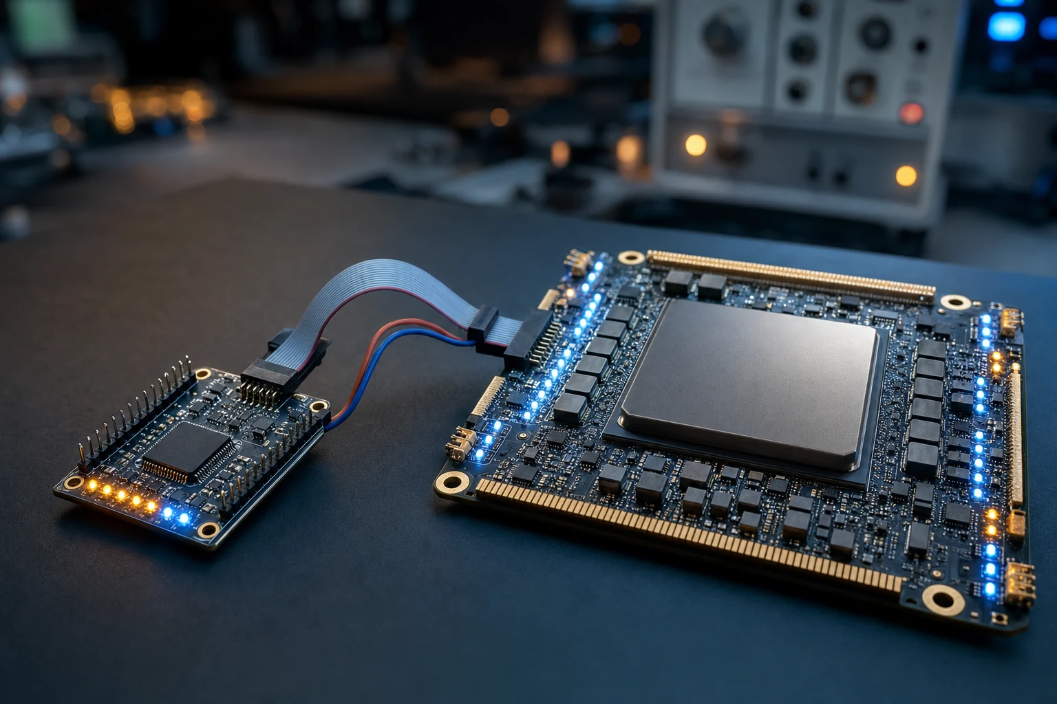
Industry news — On 26 March 2026 Espressif announced the ESP32-S31, a dual-core RISC-V microcontroller clocked at 320 MHz with 512 KB of SRAM, 60 GPIO and an integrated 1000 Mbps Ethernet MAC — a useful marker of how far a low-cost microcontroller now reaches, and therefore of where the line to an FPGA has actually moved (Espressif Systems, 26 March 2026).
In short: In an FPGA vs microcontroller decision the microcontroller is the correct default, and you should use one whenever you can — the FPGA case is not speed but four specific walls: peripheral count, provably bounded sustained bandwidth, sub-microsecond jitter, and protocols that need a serial transceiver.
The microcontroller keeps taking territory. A part that ships in volume with a gigabit Ethernet MAC on the die, hundreds of kilobytes of SRAM and two cores past 300 MHz would have been a small single-board computer a decade ago; today it is a component you solder down and program in C. That trend has a consequence nobody in the FPGA business likes to say out loud: for most embedded designs, the honest recommendation is use the microcontroller. Which makes the interesting question the inverse one. If the microcontroller keeps winning, what exactly is left on the other side of the line — and how do you recognise, early enough to matter, that your design is on that side? This article answers that for I/O-bound designs: four specific walls an MCU hits, what each one looks like on a requirements list, and where the middle ground sits.
- The short answer
- What a microcontroller actually is in 2026
- The peripheral-count wall: running out of controllers
- The sustained-bandwidth wall: bursts versus a stream
- The timing-precision wall: bounded jitter, not average speed
- The protocol wall: what an FPGA transceiver does that a pin cannot
- Where the microcontroller wins outright
- The middle ground: SoC FPGAs and an MCU with an FPGA beside it
- Constraint by constraint, and five questions that settle it
- Where this stops applying
- Frequently asked questions
The short answer
A microcontroller is the correct default for embedded I/O, and a modern
one is astonishingly capable: a CPU core plus hardened UART, SPI, I2C, CAN, USB, ADC, timer, DMA and
sometimes Ethernet peripherals on a single die, programmed in C, debugged over SWD, supported by a
mature toolchain and a large hiring pool. Choose an FPGA only when the design hits one of four
walls, and be specific about which. Countability: you need more instances of a
peripheral than the part provides. Sustained bandwidth: a continuous stream that
must never drop a sample, not an impressive burst. Timing precision: a
jitter-bounded response measured in clock cycles rather than an interrupt latency measured on
average. Protocol class: PCIe, SATA or 10G Ethernet, which need a serial
transceiver and a hardware protocol engine no pin can bit-bang. If none of those applies, the MCU
wins on cost, power, schedule and staffing, and choosing an FPGA anyway is an expensive way to make
a point.
What a microcontroller actually is in 2026
A microcontroller is a processor core surrounded by a fixed menu of hardened peripheral blocks,
with its flash and SRAM, on one die. That description has not changed since the 1980s; what has
changed is how much is on the menu and how fast the core runs it. A mainstream part today typically
carries several UARTs, several SPI and I2C controllers, CAN or CAN FD, USB device and sometimes
host, a multi-channel ADC with a sequencer, capture-compare timers, and a
direct memory access controller that can move bytes between a peripheral and memory
without the core touching them. Higher-end parts add an Ethernet MAC, a memory controller for
external SDRAM, and a second core.
The news item at the top of this article is a fair marker of the ceiling: a dual-core RISC-V part
at 320 MHz with 512 KB of SRAM, 60 GPIO and a gigabit MAC, sold as a low-cost component
rather than a specialist device. Anyone drawing the FPGA line where they drew it in 2015 is drawing
it in the wrong place.
The properties that make it the default are not really technical. It is programmed in C by
engineers who already know C; its debug story is a two-wire connector and a cheap probe; its
peripherals arrive with vendor drivers, an RTOS port and years of forum answers. A functional
prototype exists in a fortnight, because the part vendor has already proved the peripherals work
together. Nothing in an FPGA flow competes with that, and pretending otherwise is how projects get
sold an FPGA they did not need. If FPGAs are new to you, our
practical primer for system
designers covers what the device actually is.
One boundary is worth clearing away in a single paragraph, because a companion article owns it. A
microcontroller executes instructions in time, one after another; an FPGA lays circuits out in
space, so independent work runs concurrently rather than taking turns. That distinction —
spatial against temporal parallelism — is the whole argument when the opponent is a
general-purpose application processor chewing through a compute problem, and we make it at length in
FPGA vs CPU: when hardware parallelism
wins. It is not the argument here. In an I/O-bound embedded design, the four walls
below bite long before raw compute does, and they bite for reasons a faster core does not fix.
The peripheral-count wall: running out of controllers
The first wall is not a performance limit at all; it is a counting limit, and it is the single
most under-appreciated reason designs move to an FPGA. A microcontroller gives you a fixed menu:
three SPI controllers, two I2C, one CAN, one Ethernet MAC. That is not a budget you can spend
differently — it is silicon that was taped out with those blocks and no others. When the
requirement says sixteen synchronous ADC channels, twelve ARINC 429 receivers or eight
simultaneous SATA links, no clock-speed increase helps. You have not run out of throughput. You have
run out of instances.
The workarounds are familiar and each has a ceiling. Bit-banging a fourth SPI port costs core time
and gives up the peripheral’s timing guarantees. An external multiplexer serialises what the
specification wanted in parallel — fine for configuration registers, fatal for synchronous
sampling. Two microcontrollers with a link between them turn one timing problem into three. All are
reasonable at the margin, and all are how a design ends up with firmware nobody wants to own.
An FPGA answers differently: a peripheral controller is a block of logic, and you instantiate as
many as the fabric holds. That is literally how the IP is parameterised. The Logic Design Solutions
M429GEN ARINC 429 core has independent receivers and transmitters each with
FIFOs, and its feature list states the “Number of RX and TX line defined by Generics”.
Twelve receivers is a parameter change and a resource check, not a redesign, and every receiver runs
concurrently with its own FIFO and its own interrupt. The legacy macros in the same family show the
same shape frozen at fixed sizes — M429T1R1 with one receiver and one transmitter, MEF4442A
with four and one, M68C429A with eight and three — which is the menu problem solved once per
part number instead of once per project. We cover the core in our article on the
ARINC 429 IP core for an FPGA avionics
data bus.
The same applies to ordinary glue. The LDS serial macro family — MI2CM, MI2CS and MI2CMS
for I2C, MSPIM and MSPIS for SPI, MUART, M16550 and M16450 for asynchronous serial — ships as
VHDL source and is instantiated per port. The I2C masters are described as compliant with the
I2C-bus specification, standard mode at 100 Kbits, with 7-bit and 10-bit addressing and a
hardware digital filter on SCL and SDA, running at a “system clock up to 180 MHz”
subject to FPGA speed grade. The SPI master is stated to be “capable of high speed serial data
transfer with up to 8 SPI slave”; the SPI slave is quoted at up to 220 MHz, the M16450
UART at up to 150 MHz, and the M16550 at “Up to 1M baud (system frequency
dependent)”. Whether you need one of each or nine of one is a fabric question. Our
companion piece on I2C, SPI and UART IP cores
as FPGA glue logic goes through the family properly.
The sustained-bandwidth wall: bursts versus a stream
Sustained bandwidth is a different property from peak bandwidth, and conflating the two is how
data-acquisition projects fail late. A microcontroller’s DMA engine can move a genuinely impressive
burst: it fills a buffer from an ADC or a serial port while the core does something else, and the
datasheet number is real. A continuous ingest is a different problem. Every byte that arrives has to
leave the buffer as fast as it arrives, forever, with no pause where the core catches up.
The maths is qualitative but unforgiving. Let the input rate be whatever your sensors produce and
the output rate be whatever the sink — a drive, a link, a memory — can absorb. If the
output exceeds the input at every instant, buffer depth stays bounded and you can prove it. If the
output merely averages higher, buffer occupancy is a random walk and the question becomes
how long the worst-case stall lasts. On a microcontroller that stall is software: a handler that ran
long, a flash write that blocked the bus, a cache miss, a scheduling decision. Each is bounded in
practice and awkward to bound on paper — and a design is provable when you can put a
number on maximum buffer depth, which software turns into an argument rather than a
calculation.
Continuous recording to storage is the canonical case. A recorder writing to SATA or NVMe must
sustain its rate across the drive’s own behaviour: garbage collection, cache flushes, queue depth.
An FPGA implementation puts the whole chain in logic — capture, buffer, file system or raw
block addressing, protocol engine — so the bound is a property of the pipeline rather than of
a scheduler. The LDS SATA III recorder line, covered in
SATA III recorder IP for
continuous high-rate logging, writes FAT32 or raw sectors, supports RAID0 across multiple disks
and handles jumbo frames up to 9216 bytes on its Ethernet side; the NVMe equivalent is in
NVMe host recorder IP for
high-speed data acquisition, with eight namespaces, up to sixteen independent I/O queues and
sector sizes of 512 bytes or 4096 bytes.
The only measured throughput figure Logic Design Solutions has ever published is roughly
500 MBytes/sec on a single 6 Gbit SATA link, in a 2019 news announcement. It is quoted
here because it is the one number that exists; everything else — Gen4 and Gen5 NVMe rates,
per-device resource utilisation, latency — is unpublished and is not estimated here. Ask for
figures against your device, configuration and drive, and treat anything you have not received in
writing as unknown.
The timing-precision wall: bounded jitter, not average speed
Interrupt latency on a microcontroller is variable by construction, and the variability is the
wall, not the latency. When an event asserts, the core finishes or abandons its current instruction,
saves context, resolves priority against other pending interrupts, vectors to the handler, and only
then runs your code. Each step is fast; their sum depends on what the core was doing, whether a
higher-priority handler is active, whether the instruction was a multi-cycle memory operation and
whether the code was in cache. Vendors publish worst-case figures for a reason: the spread is the
specification, not the mean.
For most control loops that is irrelevant — motor commutation, a PID at a few kilohertz, a
protocol with a millisecond turnaround, and the jitter disappears into the margin. The wall appears
when the response must occur inside a window measured in hundreds of nanoseconds, when two events
must be timestamped against each other with sub-microsecond confidence, or when an output must
assert a precise number of cycles after an input edge every single time.
An FPGA pipeline has a fixed latency in clock cycles, the same on the first event and the
ten-billionth, because there is no context to save, no priority to arbitrate and no software in the
datapath. That property — determinism, not speed — is what buys the timing argument, and
it is what makes the design reviewable: timing analysis over a synchronous pipeline produces a
bound, whereas the same argument over an interrupt handler produces a measurement campaign. In
regulated domains it matters twice over, which is why LDS states that DO-254 design, verification
and traceability documentation is available on request for cores such as MSPIM, MSPIS, MUART and the
ARINC 429 family.
The protocol wall: what an FPGA transceiver does that a pin cannot
Some interfaces are simply out of reach of a general-purpose I/O pin, and no amount of firmware
changes that. PCI Express, SATA and 10 Gigabit Ethernet are multi-gigabit differential
serial links. They need a serial transceiver — a hardened analogue block with a
clock-data recovery loop, programmable equalisation and pre-emphasis, and a serialiser running at
the line rate — and above it a protocol engine implementing line coding, framing, ordered
sets, link training, flow control and error handling in hardware. You cannot bit-bang any of it. The
signal integrity requirements alone put it outside what a CMOS GPIO driver can do.
This is why an FPGA with transceivers is qualitatively, not quantitatively, different from a
microcontroller. AMD, Altera and Microchip all ship families with hardened transceiver tiles and, on
many parts, hardened PCIe controllers beside them; the fabric then carries the protocol layers the
hard block does not. That arrangement is what makes an NVMe host, a SATA host or a 10G MAC practical
in an FPGA, and it has no equivalent in the microcontroller world beyond the specific interfaces a
part vendor chose to harden. For how the PCIe side fits together — endpoint against root
complex, and why an NVMe host needs the latter — see
PCIe on FPGA explained.
The practical test is blunt: look down the interface list and ask whether any entry requires a
transceiver. If one does, the debate is over. If none does — if the list is UART, SPI, I2C,
CAN, ADC and GPIO — this is not the wall you are hitting, and the other three deserve an
honest check before you spend the FPGA premium.
Where the microcontroller wins outright
There are six places where the microcontroller wins and no FPGA argument survives contact with
them. Saying so plainly is the point of this article.
- Unit cost. At volume, a microcontroller with the peripherals you need is
cheaper than an FPGA with the fabric to build them, usually by a wide margin. - Power at low duty cycle. Microcontrollers are built around sleep: a part that
wakes on a timer, samples, transmits and sleeps spends most of its life drawing microamps. FPGA
fabric and its configuration are powered regardless of activity, and while flash-based families cut
the static component, they do not turn an FPGA into a coin-cell part. - Time to first prototype. A fortnight to a working board running C, against a
synthesis, place-and-route and timing-closure flow with its own vocabulary. On a schedule-driven
project this is often the whole decision. - Firmware update simplicity. Shipping a new binary to a fleet is a solved
problem: bootloaders, dual-bank flash, rollback. Field-updating a bitstream is routinely done, but
it is a larger image, a longer write and a more consequential failure mode. - Certification precedent. Regulated industries hold decades of practice for
microcontroller software — coding standards, tool qualification, test strategies, auditors who
have seen it before. Hardware design assurance is well defined too, but the precedent base is
narrower and the specialists scarcer. - Hiring. You can recruit an embedded C engineer next month. An experienced VHDL
or Verilog engineer takes longer, costs more, and leaves you with a design only that person
understands unless you plan against it. That is an engineering constraint, not an excuse.
None of that argues against FPGAs. It argues for using one deliberately, because a requirement
forced it.
The middle ground: SoC FPGAs and an MCU with an FPGA beside it
The choice is not binary, and most shipping systems live between the two poles. An
SoC FPGA puts a hardened processor subsystem and programmable fabric on the same die:
AMD’s Zynq 7000 and Zynq UltraScale+ MPSoC, Altera’s Agilex SoC and Arria SoC families, and
Microchip’s PolarFire SoC and SmartFusion2. The hard processor runs Linux or an RTOS and handles
configuration, networking, user interface and anything that is genuinely software; the fabric
handles the counted peripherals, the deterministic pipeline and the transceiver-class interfaces.
The two talk over an on-chip bus, and the architectural work is deciding what belongs on which side.
That split is not free: you own two toolchains, a hardware-software interface to specify and
version, and a debug story spanning both. It buys a great deal when the design needs both halves,
and it is overhead when it does not.
The other common architecture deserves saying explicitly because it is often the cheapest correct
answer: a microcontroller plus a small FPGA beside it on the board, the FPGA acting
as an I/O expander and pre-processor. The FPGA instantiates the twelve receivers, the sixteen
synchronised ADC front ends or the eight serial ports, does the timing-critical work and the
decimation or framing, and presents the MCU with a manageable summary over a bus it already has. The
application stays in C where the team is productive; only the countable, jitter-sensitive part
crosses into fabric. Small flash-based and low-cost SRAM-based FPGAs from all three vendors are
sized for exactly this role, and LDS delivers its cores as VHDL source with C drivers so the fabric
side and the processor side can be integrated by one team. Choosing the device family is its own
exercise — our note on
choosing an FPGA across AMD,
Altera and Microchip walks through the criteria.
Constraint by constraint, and five questions that settle it
Each row below is a constraint from a real requirements list, not a benchmark. The winner column
is the default given that constraint alone; a real design weighs several at once, and one hard
constraint usually dominates all the soft ones.
| Constraint | Winner | Why |
|---|---|---|
| Channel count beyond the part’s menu | FPGA | A controller is a parameterised block instantiated as many times as the fabric holds; an MCU’s peripheral set was fixed at tape-out and cannot be spent differently. |
| Sustained ingest rate with no dropped samples | FPGA | Buffer depth can be bounded by construction over a synchronous pipeline; on an MCU the bound depends on worst-case software behaviour you have to measure rather than derive. |
| Response jitter below a microsecond | FPGA | Pipeline latency is a fixed number of clock cycles on every event; interrupt latency varies with core state, priority and cache. |
| Protocol class needing a serial transceiver | FPGA | PCIe, SATA and 10G Ethernet require a hardened transceiver plus a hardware protocol engine. No GPIO can produce those signals at any clock speed. |
| Unit cost at volume, requirements already met | Microcontroller | An MCU that fits the menu is materially cheaper than fabric sized to rebuild the same peripherals. |
| Time to market on a fixed date | Microcontroller | C on a supported part with vendor drivers reaches a working prototype far sooner than a synthesis and timing-closure flow, and the risk profile is better understood. |
| Power budget with a low duty cycle | Microcontroller | Deep sleep modes dominate average consumption; FPGA fabric and its configuration are powered regardless of activity. |
| Both halves genuinely required | SoC FPGA, or MCU plus small FPGA |
Software-shaped work stays on a processor; counted, timed and transceiver-class work goes to fabric, with one bus between them. |
Five questions that resolve the decision
- Count every channel, then add the ones marketing will ask for. Write the total
beside what your candidate part actually provides. If it exceeds the menu, that is a countability
problem and no faster part fixes it. - Multiply worst-case sample rate by worst-case payload, and ask where every byte
exits. If you cannot name a sink faster than the source at every instant, you are relying
on buffering and need a bound on buffer depth before choosing a device. - Write the worst acceptable jitter down as a number. Tens of microseconds: a
microcontroller with a well-designed interrupt scheme will do. Sub-microsecond, holding every time:
plan for fabric. - Does any interface need a serial transceiver? PCIe, SATA, 10G Ethernet and
their relatives end the debate on their own. UART, SPI, I2C, CAN, ADC and GPIO do not. - Who maintains this in five years, and at what volume? Unit cost, hiring pool
and update strategy are engineering constraints. An architecture nobody on the team can modify is
not superior.
If questions one to four all answer in the microcontroller’s favour, use a microcontroller. That
is the honest recommendation, it is right most of the time, and a vendor who cannot say it is not
worth asking about the cases where it is wrong.
Tell us the interface list, the channel counts and the worst-case sustained rate you have to hold, and we will tell you honestly whether it belongs in a microcontroller, in fabric, or split across both.
Where this stops applying
This comparison is scoped to I/O-bound embedded designs and to the walls a microcontroller hits
in that context. The boundaries:
- Compute-bound problems are a different argument. If your bottleneck is signal
processing, inference or cryptography rather than interfaces, the relevant comparison is against a
CPU or a GPU, and the reasoning runs through spatial parallelism rather than peripheral counts. - No device figures are compared here. This article names no MCU or FPGA resource
count, power figure, interrupt latency or throughput number for a specific part, because those
belong to a datasheet you must read for the candidates in front of you. Every device claim here is
attributed to its vendor. - No LDS core performance is published. Resource utilisation, maximum frequency,
latency and design assurance level are not in the public material for any LDS IP, and nothing here
estimates them. The single published throughput figure is roughly 500 MBytes/sec on one
6 Gbit SATA link, from 2019. - Microcontroller capability is a moving target. The ESP32-S31 announcement is a
2026 marker, not a permanent boundary. Parts with more hardened interfaces ship every year, and the
line moves in the microcontroller’s favour each time. Re-check the menu, do not rely on memory. - Certification is a programme, not a device choice. DO-254 documentation being
available on request for an IP core is an input to a certification effort, not a substitute for one,
and the design assurance level applicable to your system is set by your authority.
In summary
A modern microcontroller is a remarkable piece of engineering and the right default
for most embedded I/O, and any comparison that does not start there is selling something. The FPGA
case is not that the microcontroller is slow. It is that four specific requirements have no
microcontroller answer: more instances of a peripheral than the part provides, a stream whose buffer
depth must be provably bounded, a response whose jitter must be measured in clock cycles, and a
protocol that needs a serial transceiver and a hardware engine above it.
Those walls are recognisable early if you count channels, multiply rates, write the jitter budget
down as a number and check the interface list for transceiver-class links. Where one or two of them
bite and the rest of the system is ordinary software, the answer is usually not a pure FPGA at all
but an SoC FPGA from AMD, Altera or Microchip, or a microcontroller with a small FPGA beside it
absorbing the counted and timed work. Logic Design Solutions builds the fabric side of exactly those
architectures — ARINC 429, I2C, SPI and UART controllers instantiated per channel, and
SATA, NVMe and 10G Ethernet cores for the transceiver-class links — delivered as VHDL source
with C drivers so the processor side and the logic side stay one design.
Frequently asked questions
What is the main reason designs move from a microcontroller to an FPGA?
Peripheral count, more often than raw speed. A microcontroller ships with a fixed menu of controllers decided at tape-out — three SPI, two I2C, one Ethernet MAC — and a design needing sixteen synchronous ADC channels or twelve ARINC 429 receivers has hit a countability limit that no clock-speed increase addresses. In an FPGA a controller is a parameterised logic block you instantiate as many times as the fabric holds, which is why LDS defines its ARINC 429 receiver and transmitter line counts by VHDL generic rather than by part number.
Is a microcontroller ever fast enough for high-throughput I/O?
Frequently, yes, and it is the correct default. A modern part combines a fast core, DMA that moves bytes without core involvement, and hardened peripherals; the Espressif ESP32-S31 announced in March 2026 is a dual-core RISC-V microcontroller at 320 MHz with 512 KB of SRAM and an integrated gigabit Ethernet MAC. The distinction that matters is peak burst against sustained stream: if every byte must leave the buffer as fast as it arrives, forever, the bound on buffer depth is the thing to prove before choosing a device.
Why can a microcontroller not implement PCIe, SATA or 10G Ethernet in software?
Because those are multi-gigabit differential serial links that require a hardened transceiver with clock-data recovery, equalisation and pre-emphasis, plus a hardware protocol engine handling line coding, framing, ordered sets and link training. A general-purpose CMOS output driver cannot produce those signals at any clock speed, so no amount of firmware substitutes for the analogue block. AMD, Altera and Microchip all ship FPGA families with transceiver tiles and, on many parts, hardened PCIe controllers beside them.
How much better is FPGA timing than a microcontroller interrupt?
The useful difference is jitter, not average latency. An FPGA pipeline responds after a fixed number of clock cycles on the first event and on the ten-billionth, because there is no context to save and no other software competing for the datapath. A microcontroller interrupt varies with core state, pending priorities, memory access and cache behaviour, which is why vendors publish worst-case rather than typical figures. This article gives no comparative numbers: read them from the datasheets of the parts you are actually considering.
Should I use an SoC FPGA instead of choosing between the two?
Often, yes. AMD Zynq and Zynq UltraScale+, Altera Agilex SoC and Arria SoC, and Microchip PolarFire SoC and SmartFusion2 place a hardened processor subsystem beside programmable fabric on one die, so software-shaped work stays in software and counted, timed or transceiver-class work goes to logic. The cost is two toolchains and a hardware-software interface to specify and version. A microcontroller with a small FPGA beside it on the board achieves a similar split at board level and is often the cheaper correct answer.
Which throughput figures has Logic Design Solutions published for its cores?
One. A 2019 announcement records roughly 500 MBytes/sec on a single 6 Gbit SATA link. No resource utilisation, maximum frequency, latency or design assurance level is published for any LDS core, and nothing in this article estimates them. Published device-level facts do exist and are quoted here — I2C masters at a system clock up to 180 MHz, the SPI slave up to 220 MHz, the M16450 UART up to 150 MHz, ARINC 429 up to 2.5 Mbit/s — but they are frequency and rate limits, not measured throughput.
- Espressif Systems — ESP32-S31 announcement, 26 March 2026: the dual-core RISC-V microcontroller at 320 MHz with 512 KB SRAM, 60 GPIO and an integrated 1000 Mbps Ethernet MAC cited in the opening.
- AMD — Zynq UltraScale+ MPSoC: vendor documentation for the AMD SoC FPGA family that places a hardened processor subsystem beside programmable fabric.
- Altera — Agilex FPGA and SoC families: vendor documentation for the Altera SoC FPGA and transceiver-equipped families named in this article.
- Microchip Technology — PolarFire SoC FPGAs: vendor documentation for the Microchip SoC FPGA family, the low-static-power option in the middle-ground architectures.
- PCI-SIG — PCI Express Specifications: the standards body defining the serial link and protocol layers that put PCIe beyond any microcontroller GPIO.
- SATA-IO — Serial ATA International Organization: the body defining SATA, including the 6 Gbit link referenced in the one published LDS throughput figure.
- AEEC / SAE-ITC — ARINC Industry Activities standards: the committee that publishes the ARINC 429 specification implemented by the LDS M429GEN core.
- Logic Design Solutions — ARINC 429 IP product page: the M429GEN feature list quoted here, including receiver and transmitter line counts defined by generics and support up to 2.5 Mbit/s.
- Logic Design Solutions — MI2CM I2C master macro product page: the I2C master feature list quoted here, including standard mode at 100 Kbits, 7-bit and 10-bit addressing and a system clock up to 180 MHz.