
News : In November 2024, Infineon introduced a radiation-hardened 512 Mbit quad-SPI NOR flash, rated for 300 krad(Si) total ionising dose and qualified to QML-V and QML-P, with configuration image storage for space-grade FPGAs as a typical use. For FPGA storage IP, it is a reminder that qualification covers every memory in the chain, configuration storage included. (Electronics Weekly, 18 November 2024).
Radiation flips bits. Temperature swings shift voltages. A single metastable signal can corrupt stored data. The cited sources report proton radiation test results at PSI and describe NASA’s TID method for measuring propagation delay between flip-flops operating at maximum speed.
This guide reviews the published test methods and the design rules that keep storage IP predictable under those conditions: radiation testing, core power, file system choice, Block RAM access and validation before hardware exists.
The short answer
Qualify space-grade FPGA storage IP by matching test protocols to the mission profile. Proton testing, as done at PSI in the EU OPERA project, and NASA’s TID method, which tracks propagation-delay degradation between flip-flops at full speed, are two documented references. Describe Block RAM with synchronous reads in RTL, and pick the FAT variant the host must read: UEFI firmware supports FAT12, FAT16 and FAT32. For high-current core supplies, look for differential remote sensing, as in the ISLVERSALDEMO2Z reference design for Versal (up to 140 A). Validate communication stacks with FPGA-in-the-loop testing before RF hardware exists, and consider a RISC-V soft core when spare FPGA capacity is available.
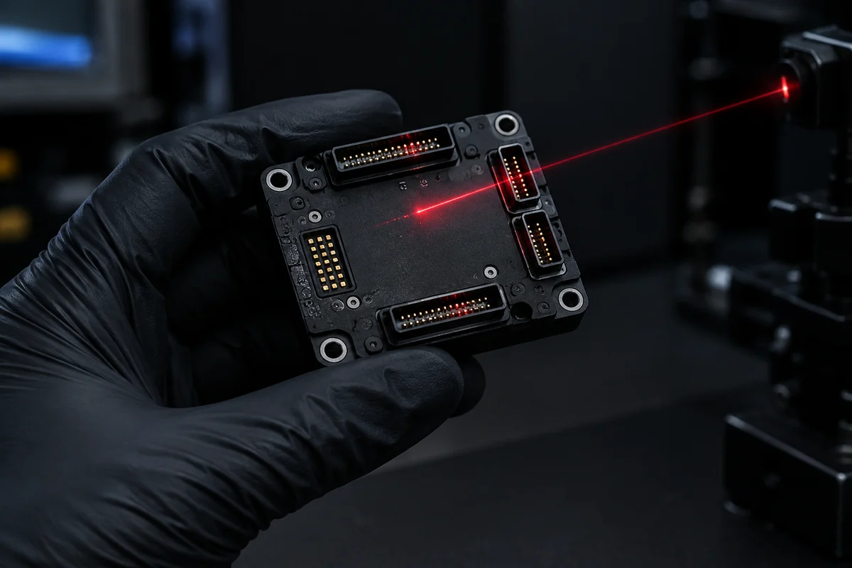
Key radiation testing protocols for space-grade FPGA storage IP
Proton and total ionizing dose (TID) tests can help assess radiation hardness.
The EU OPERA project, which qualifies a high-performance European rad-hard FPGA, lists among its deliverables a report on proton radiation test results done at PSI.
NASA researchers proposed a TID test method that measures the delay between flip-flops while the FPGA runs at full speed, instead of timing a single input-to-output path, as described in their paper. The measured degradation can then be built into timing margins for the predicted dose.
For space applications, ask for documented proton and TID test results for the FPGA and memories that host the storage IP.
How space-grade FPGAs handle high-current core voltage requirements
Renesas’ ISLVERSALDEMO2Z reference design can supply up to 140 A to AMD’s space-grade Versal devices.
In July 2023, Renesas presented the ISLVERSALDEMO2Z reference design, which generates a 0.80 V core supply for Versal devices and can source up to 140 A of current.
The design has a -55 °C to +125 °C operating range and differential remote sensing of the output voltage, which compensates for the voltage drop between regulator and load.
For high-current designs, prioritize power solutions with remote sensing to hold voltage accuracy under dynamic loads.
Core voltage requirements vary by device family. The table below summarizes the published figures of this reference design:
| Parameter | ISLVERSALDEMO2Z (Versal) |
|---|---|
| Core voltage | 0.80 V |
| Maximum current | 140 A |
| Operating temperature | -55 °C to +125 °C |
| Remote sensing | Differential |
FAT16 file system implementation for FPGA-based micro-SD storage
A FAT16 file system on FPGA-based micro-SD storage is readable by UEFI firmware and keeps the on-disk structure simple.
The UEFI specification requires EFI firmware to support FAT32, FAT16, and FAT12. For small removable media in radiation-tolerant designs, we prefer FAT16 because its simpler layout is easier to verify; that is our opinion, not a requirement.
In FAT16 the root directory lies outside the cluster area and has a fixed size, unlike FAT32, as course materials from the University of Massachusetts explain; that fixed root directory is typically limited to 512 entries. When more entries are needed, subdirectories add them without changing the file system’s core behavior.
microSD cards have 8 pins in their High Speed and UHS-I versions, according to the SD Association, which keeps routing compact on space-constrained boards.
We recommend FAT16 for small removable media when the host reads it through UEFI firmware and the file count is modest.
Key differences between FAT16 and FAT32 for FPGA storage:
| Feature | FAT16 | FAT32 |
|---|---|---|
| Root directory location | Outside cluster area | Within cluster area |
| Root directory size | Fixed, typically 512 entries | Grows as a cluster chain |
| UEFI firmware support | Required | Required |
Synchronous Block RAM access requirements in space-grade FPGAs
Describe Block RAM with synchronous reads so that synthesis maps it to Block RAM, whatever the clock speed.
Synchronous access aligns read and write operations with the clock edge. A 2003 comp.arch.fpga thread on a Spartan II design clocked at 24 MHz shows the failure mode: a RAM that worked in simulation behaved as if it were absent in hardware, while the synthesis tool warned that only a synchronously read RAM description can be implemented in Block RAM. The requirement isn’t about speed: it’s about predictability.
For space-grade designs, this rule tightens. Radiation-induced upsets can flip bits in control logic. Synchronous access does not prevent single-event upsets, but registered interfaces make the design easier to time, protect and verify.
Our advice: enforce synchronous access in your RTL, even for low-speed interfaces. Use the FPGA’s built-in clocking resources to generate clean, phase-aligned signals. For example, Altera’s Phase-Locked Loops (PLLs) can deskew signals and generate multiple clock domains, but they require explicit configuration in the design constraints. Skip this step, and you risk silent data corruption: especially in space, where debugging is very limited.
If your design mixes clock domains, use synchronizers for control signals. A two-flop synchronizer adds minimal latency (one clock cycle) but prevents metastability from propagating. For data buses wider than 8 bits, consider using a FIFO with built-in synchronization.
| Access Type | Risk in Space-Grade FPGAs | Recommended Fix |
|---|---|---|
| Asynchronous read/write | Metastability, SEU-induced corruption | Enforce synchronous access in RTL |
| Mixed clock domains (no synchronizer) | Signal misalignment, data loss | Use two-flop synchronizers or FIFO IP |
| Unconstrained timing paths | Setup/hold violations at low speeds | Apply timing constraints in SDC files |
For storage IP, synchronous access isn’t optional: it’s a baseline. Logic Design Solutions’ IP cores are delivered as source code, so the clocking scheme can be reviewed directly, and your integration must match it. If you’re adapting third-party IP, check the datasheet for clocking requirements. Some cores assume a single clock domain; others support multiple but require explicit synchronization. Ignore this, and your storage system may work in simulation but fail in orbit.
When to use RISC-V processors instead of FPGA storage IP for space applications
For space applications, a RISC-V soft-core processor can take over simple storage tasks when spare FPGA capacity exists and storage needs are modest.
When the FPGA still has unused logic and memory blocks, a soft-core processor can replace a discrete processor. This works best for sequential operations at lower speeds, where simplicity matters more than throughput.
However, when the mission demands sustained high-speed transfers, deterministic latency, or hardware error correction, dedicated FPGA storage IP is the better fit. The spare capacity that could host a RISC-V core can instead hold FIFO controllers, DMA engines and scrubbing logic, which a soft core would run in software, more slowly.
Southwest Research Institute’s NOEL-V project found it “now feasible to implement an advanced softcore microprocessor within the FPGA itself”, with the potential to reduce part count while making efficient use of spare FPGA capacity, according to SwRI. We recommend this trade-off when the storage workload fits within the remaining capacity and part count matters more than peak performance.
| Decision factor | RISC-V soft-core | FPGA storage IP |
|---|---|---|
| Part count | Reduces external components by using spare FPGA capacity | Requires dedicated storage controllers |
| Throughput | Best for sequential, low-speed operations | Handles sustained high-speed transfers |
| Latency | Variable, software-dependent | Deterministic, hardware-controlled |
| Error correction | Limited to software implementations | Can be implemented in hardware |
If the FPGA’s spare capacity is minimal or the workload exceeds the soft core’s capabilities, dedicated FPGA storage IP is the safer choice.
Automated FPGA-in-the-loop testing pipelines for 5G NTN stacks
Automated FPGA-in-the-loop pipelines let teams validate 5G NTN stacks before satellite hardware is ready.
For 5G non-terrestrial network (NTN) stacks, automated FPGA-in-the-loop testing shortens the wait for full satellite hardware. ESA’s FPGA rapid prototyping project for 5G builds on the SpaceStudio environment, targets Xilinx Zynq, UltraScale+ and Versal boards, and plans an automated deployment pipeline for FPGA-in-the-loop testing on Versal boards.
Our advice: use Versal boards for high-bandwidth NTN stacks.
These pipelines also simplify integration. When the storage IP is delivered as source code, as LDS cores are, teams can include it in the same FPGA-in-the-loop setup and test protocol and storage together before launch.
In summary
Ask for proton and TID test data on the devices that host your storage IP before integration. Verify synchronous Block RAM access in your RTL, even for low-speed interfaces, and enforce timing constraints in SDC files. For high-current designs, use power solutions with differential remote sensing to compensate for voltage drops.
Now, map your mission’s radiation profile to the test data. If the devices and IP meet it, proceed to FPGA-in-the-loop validation for 5G NTN stacks or edge-case stress tests. If not, revisit the RTL or choose a device with the required radiation data.
How we wrote this article
The sources we consulted are listed at the end of the article, consulted on 1 October 2026. Where we cite none, it is our opinion, and we write it as such.
This article gives buying criteria and our point of view. It does not replace a professional’s advice on a specific situation.
It is published by Logic Design Solutions, which therefore has an interest in the subject.
Sources
- Full power management design for AMD’s space grade Versal SoC …, eenewseurope.com
- comp.arch.fpga | Spartan II Block Ram, fpgarelated.com
- FPGA Rapid Prototyping Methodology for 5G – ESA CSC: Connectivity & Secure Communications, resilience.esa.int
- Space Qualification and Validation of High Performance European Rad-Hard FPGA | OPERA | Project | Results | H2020 | CORD, cordis.europa.eu
- A Robust Strategy for Total Ionizing Dose Testing of Field Programmable Gate Arrays – NASA Technical Reports Server (NTR, ntrs.nasa.gov
- 11: FATs and Directory Entries | COMPSCI 365 | Digital Forensics (Spring 2019), people.cs.umass.edu
- NOEL-V Processors for Spaceflight Embedded Platforms, 10-R6129 | Southwest Research Institute, swri.org
- Products – Logic Design Solutions | Logic Design Solutions, logic-design-solutions.com