Industry news — On 2 March 2026 the Accellera Systems Initiative approved its Standard for IP Abstraction for Clock and Reset Domain Crossing Integration 1.0, a vendor-neutral way to capture and exchange CDC/RDC intent so a core’s clock- and reset-crossing analysis travels with the IP instead of being re-run, and re-argued, in every integrator’s tool chain (Accellera Systems Initiative, 2 March 2026).
In short: serious FPGA verification services for storage and bus IP run four layers — simulation, protocol compliance against the published spec, hardware-in-the-loop bring-up on real devkits and real drives, and a regression suite that keeps all of it true after the next commit.
That announcement illustrates where verification effort actually goes on a storage or bus core. Nobody spends weeks on the happy path: a SATA link that comes up, an NVMe read that returns the right sector, an ARINC 429 label that decodes. Those work on day three. The weeks go into the domain crossings, the error paths, the drive that answers later than the last one, and the power cut in the middle of a write. This article sets out what a rigorous programme looks like stage by stage, what each stage catches, and which deliverables you should expect — so you can tell a real verification effort from a demo that happened to pass.
- The short answer
- What verification means when the IP is storage or a bus
- The verification stages, and what each catches
- Simulation: where most bugs should die
- Protocol compliance: SATA, NVMe, ARINC 429
- Hardware-in-the-loop: real devkits, real SSDs
- Corner cases: error injection, power loss, thermal
- Deliverables a verification service should hand over
- Why a vendor who verifies its own cores de-risks your programme
- Where this stops applying
- Frequently asked questions
The short answer
FPGA verification services for storage and bus IP mean four things done in order. Simulation with directed and constrained-random stimulus, protocol assertions and a coverage model, to kill logic bugs cheaply. Compliance checking against the published specification — Serial ATA, NVM Express, ARINC 429, AMBA AXI — clause by clause, so “it works” becomes “it conforms”. Hardware-in-the-loop bring-up on a named development board with named drives, because real PHYs and real SSD firmware do things no model does. And a regression suite that re-runs the lot on every change and every new device family. Everything else — error injection, power-loss testing, thermal soak, timing closure — hangs off those four.
What verification means when the IP is storage or a bus
Verifying a compute block is mostly about arithmetic: given these inputs, do you get the right outputs? Verifying a storage or bus core is about protocol and time. The core is a participant in a conversation defined by a document hundreds of pages long, with a partner it did not design, over a physical link that occasionally corrupts things. Three consequences shape the whole programme.
- The specification is the test plan. A SATA host has to negotiate out-of-band signalling, align on comma characters, honour flow-control primitives, compute CRC32 over each frame and handle queued commands. Each of those is a clause you can point at, and each clause is a test you either ran or did not.
- The other end is not under your control. Two SSDs from different vendors, both conformant, differ in queue-depth behaviour, latency distribution and response to a reset mid-transfer. Verification that only ever talked to a model has verified your assumptions, not your core.
- Sustained behaviour beats any single transaction. A recorder that drops one sector in ten million is broken for its purpose — and verification has to run long enough for that event to appear at all.
That is the difference between a demonstration and a verification programme, and it is worth agreeing on before custom FPGA development starts, not after.
The verification stages, and what each catches
Each stage catches a class of defect the others structurally cannot. Skipping one does not spread its work across the rest; it leaves that class of bug in the design until it surfaces on your bench, or on a customer’s.
| Verification stage | What it catches | Deliverable |
|---|---|---|
| Specification and test-plan review | Ambiguous or untestable requirements; corner cases nobody agreed on | Verification plan mapping every requirement to a named test |
| Directed block simulation | Plain RTL bugs: state machines, counters, CRC, framing, decode | Block testbenches and pass/fail logs |
| Constrained-random stimulus and assertions | Legal-but-rare sequences nobody would write by hand; protocol rule violations | Testbench, assertion set, seed list to reproduce any failure |
| Coverage closure | What you did not test — unvisited states, untaken transitions | Functional and code coverage report with justified exclusions |
| Bus-interface checking (AXI, AXI-Lite, Avalon, APB) | Handshake violations, illegal bursts, deadlock and starvation | Bus protocol checker report per interface |
| Clock- and reset-domain crossing analysis | Metastability, missing synchronisers, reset ordering and release | CDC/RDC report with reviewed waivers |
| Protocol compliance review | Divergence from the spec: OOB sequences, queueing rules, word and label formats | Compliance matrix, clause by clause |
| Hardware-in-the-loop bring-up | What simulation cannot: real PHY behaviour, drive firmware quirks, real timing | Bring-up report naming board, device and firmware revisions |
| Error injection, power-loss and thermal soak | Recovery from CRC errors, link loss and timeouts; rare-event data loss; throughput decay under heat | Fault-class results and soak logs with duration, volume and error counts |
| Timing closure and regression | Setup/hold and constraint problems; what the last fix or the port to a new family silently broke | Timing report, constraints, and a regression suite with results history |
Simulation: where most bugs should die
Simulation is the cheapest place to find a defect and the only place you can reproduce it deterministically. A serious storage-IP testbench has three layers.
Directed tests
Written from the specification, one per behaviour you can name: initialise the link, identify the device, write a logical block and read it back, issue a queued command, handle an abort. These prove the core does what the datasheet says. They are necessary, they are finite, and they will never find the bug you did not think of.
Constrained-random stimulus and assertions
Constrained-random verification generates legal traffic within declared constraints — random transfer sizes, addresses, gaps and ready patterns — across thousands of seeds. Assertions are the protocol rules written as executable checks that fire the instant they are broken, wherever the failure occurs. The methodology layer most teams use is the Universal Verification Methodology, standardised as IEEE 1800.2 and distributed by Accellera. Randomisation finds the interleaving nobody imagined; assertions stop it passing silently.
Coverage
Coverage answers the only question that matters at sign-off: what did we not exercise? A functional coverage model over command types, transfer sizes, queue depths, error conditions and state transitions turns “we ran ten thousand seeds” into “we reached these states and not those”. Uncovered bins are either a stimulus gap or an unreachable state that deserves a written justification. A verification report with no coverage section is a report about effort, not about risk.
Have a storage or bus core — ours or someone else’s — that needs a verification programme rather than another demo? Tell us the protocol, the target family and the failure you cannot afford.
Protocol compliance: SATA, NVMe, ARINC 429
Compliance is where verification stops being about your intent and starts being about the published document. It is also the part most often skipped, because a core can pass every internal test while quietly diverging from the spec in a way that only shows up against a device you have never tried.
For Serial ATA, the surface is the layer stack: out-of-band signalling and COMWAKE at bring-up, comma alignment, link-layer primitives and flow control, CRC32 per frame, 48-bit sector addressing, PIO and DMA transfers, native command queueing, and the partial and slumber low-power states. The Serial ATA International Organization maintains the specification and an interoperability programme around it. A BIST loopback mode — present in our SATA host architecture — is the cheap way to separate a link-layer problem from a cabling or PHY problem on the bench.
For NVMe, compliance is largely the queueing model: submission and completion queues, doorbells, namespaces, sector handling at 512 bytes and 4096 bytes, and correct behaviour when several I/O queues run independently. The clause-level reference is the NVM Express specification set, on a PCI Express link whose own conformance is covered by the PCI-SIG compliance programme. Our NVMe host cores expose up to 16 independent I/O queues and 8 namespaces — so the plan has to include the multi-user cases, not one queue running flat out.
For ARINC 429 the surface is smaller but the tolerance is lower, because the destination is usually an aircraft. Word format, label handling, return-to-zero encoding, parity convention and bit rate are defined by the standard published through SAE ITC. Verification means exercising both directions independently, every parity mode, multi-label reception, FIFO overrun and interrupt generation — and, on certified equipment, producing evidence in the shape airborne electronic hardware assurance expects, per the FAA’s guidance recognising RTCA/DO-254. We supply DO-254 documentation on request across the catalogue for exactly that reason.
Hardware-in-the-loop: real devkits, real SSDs
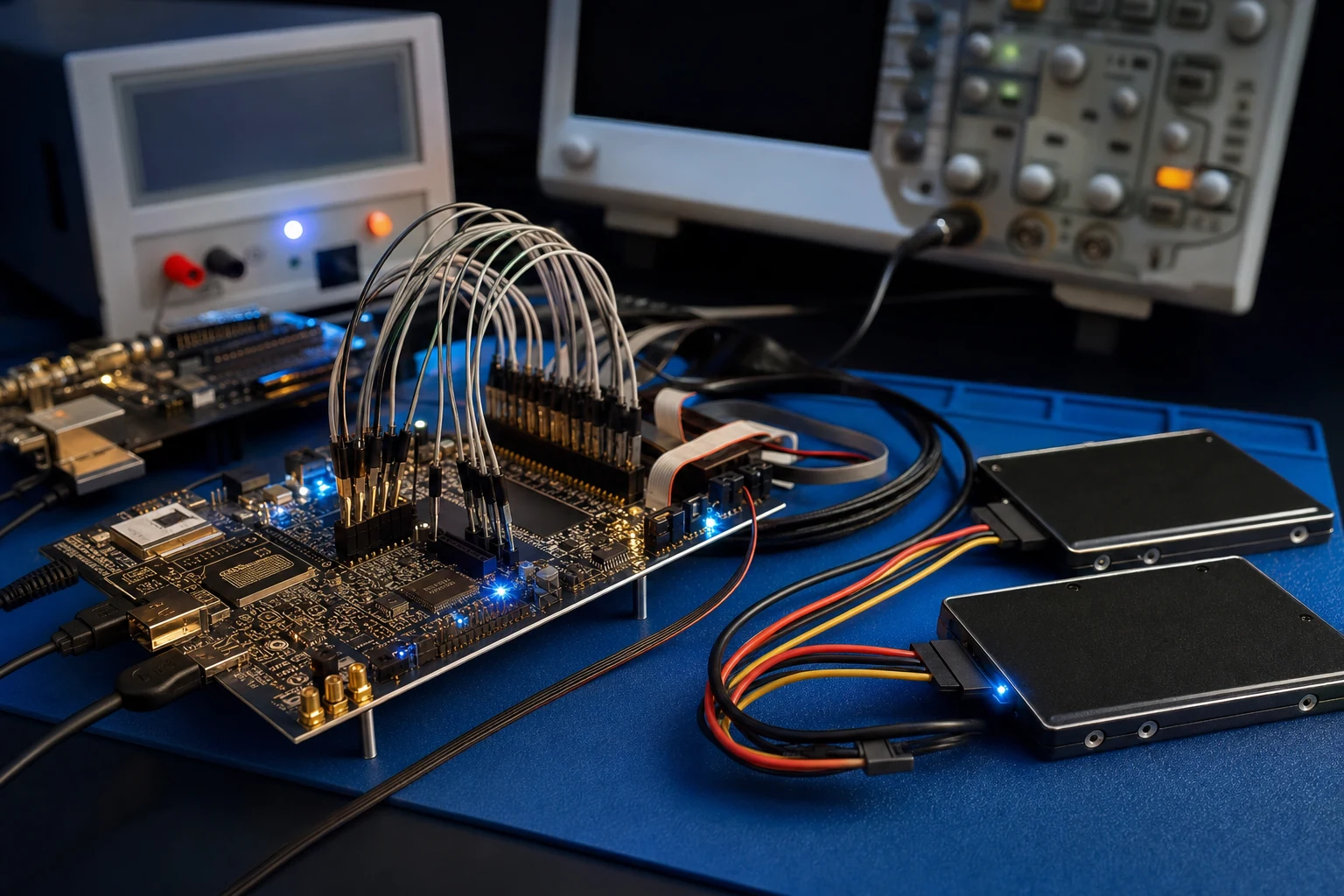
Simulation models are written from the same specification your core is. When both share a misreading, simulation agrees with you enthusiastically. Hardware-in-the-loop breaks that symmetry: the core running on a real FPGA on a named development board, driving real devices. In our own bring-up work those boards are the ones the datasheets name — KC705, VC707 and ZC706 for the earlier families, KCU105 with an FMC drive carrier, ZCU102 with an XM104, ZCU106 with an Opsero FPGADrive adapter for the newer ones — because the carrier and the connector are part of what is being verified, not incidental to it.
What this stage catches that nothing else does:
- Drive-to-drive variation. Different controllers, different firmware revisions, different latency under queue pressure. Testing against one SSD verifies compatibility with one SSD.
- Real link behaviour. Speed negotiation, retries, signal integrity through a real connector and cable, and how the core recovers when the link drops and returns.
- Sustained rate, not burst rate. Burst figures come from the interface width; sustained figures come from the drive’s steady state once its cache is full and garbage collection starts. Only hardware gives you the second number, and for a recorder it is the only one that counts.
- Long-run stability. A generator-and-checker block writing a known pattern for hours and verifying it on read-back is how you find the one-sector-in-millions fault. That block exists in our SATA recorder architecture precisely because that is the failure mode customers care about.
Corner cases: error injection, power loss, thermal
The happy path is a small fraction of the state space and none of the risk. Three families of corner case deserve explicit tests.
Error injection. Deliberately corrupt a CRC, drop a frame, force a timeout, pull the link mid-transfer, return a media error. The question is never whether the core detects the fault — detection is easy. It is what happens next: does it retry, report cleanly to your application logic, or wedge in a state only a power cycle clears?
Power loss. For a recorder, abrupt power removal during a write is a normal event, not an exception. What matters is bounded, understood damage: which sectors are committed, what the file-system layer does with a partial write, and whether the media still mounts afterwards. When an exFAT or FAT32 layer sits above the block interface, answer that at both levels — a point worth raising with any supplier, as our FPGA IP vendor checklist sets out.
Thermal and sustained load. SSDs throttle when hot, and a design validated for ten minutes on an open bench can miss its rate in a sealed enclosure. Soak testing at the intended rate, for the intended duration, in something resembling the intended environment is the only honest way to size a system.
Deliverables a verification service should hand over
Verification you cannot inspect is a claim, not evidence. A complete engagement should hand over:
- A verification plan traceable to the specification — each requirement mapped to the tests that cover it.
- The testbench itself, in source, so you can re-run and extend it. We deliver our cores as VHDL or Verilog source with C source drivers, and the same principle applies to what verifies them.
- Coverage and regression reports, with the seeds needed to reproduce any failure.
- A compliance matrix against the published protocol specification, clause by clause, including anything deliberately not implemented.
- A hardware bring-up report naming the board, the devices, the firmware revisions and the measured sustained rate on that configuration.
- Timing and constraint files for your target device, plus the CDC/RDC analysis and its waivers.
- Where relevant, DO-254 documentation in the form your certification authority expects.
If a vendor cannot produce these, the honest reading is that the work was not done, not that it was done and not written down.
Why a vendor who verifies its own cores de-risks your programme
There is a structural argument for having the same organisation write the IP, verify it and support it on your board. A core brought up across FPGA families from both vendors, against many drives, over three decades of protocol revisions, carries the result of every one of those bring-ups in its error handling. That is not a claim about cleverness; it is what happens when the people who wrote the RTL had to make it work on a bench with a customer waiting.
It also collapses the interface that usually costs the most time. When a link fails to come up the night before a milestone, the useful question is whether the problem is the core, the PHY configuration, the carrier or the drive — and one team owning all four sides answers it faster than three parties negotiating. That is the practical content of what an IP-focused design house delivers, and why verification is best scoped alongside the design rather than bolted on at the end.
Where this stops applying
This programme is the right shape for storage and bus IP on FPGA. It is not universal:
- Formal verification is a different tool. For small control blocks, arbiters and protocol checkers, formal property checking proves absence of a behaviour rather than sampling for it. It complements simulation; it does not replace hardware bring-up.
- Certification is not verification. A rigorous programme produces evidence usable in a DO-254 or functional-safety process, but the process itself — planning, independence, tool qualification, audits — is a separate discipline with its own authority. Ask what level applies to your equipment before assuming what evidence is needed.
- Numbers are device-specific. Sustained throughput, latency and LUT, FF, BRAM or DSP utilisation depend on the family, the configuration and your own timing closure. Take them from the datasheet for your exact target and your own measurements — never from a headline figure in an article, including this one.
- Interoperability is bounded by what you tested. A drive compatibility list is a list of drives that were tried. A device that has never been tested is a device whose behaviour is unknown, however conformant it claims to be.
In summary
Verification of storage and bus IP is a layered programme, not a phase. Simulation removes logic bugs cheaply. Compliance review against the Serial ATA, NVM Express, PCIe, AMBA or ARINC 429 documents turns “it works here” into “it conforms”. Hardware-in-the-loop bring-up finds what no model contains. Error injection, power-loss and thermal soak address the failures that actually cost programmes time, and regression keeps all of it true through the next fix and the next device family. Ask for the deliverables that prove each layer happened — plan, coverage report, compliance matrix, bring-up log — and the difference between a verified core and a demonstrated one is immediately visible.
Frequently asked questions
What is the difference between simulation and hardware-in-the-loop verification?
Simulation runs your RTL against a model of the other end: deterministic, reproducible, cheap, and ideal for logic bugs and protocol rule violations. Hardware-in-the-loop runs the compiled design on a real FPGA against real devices, the only way to expose PHY behaviour, drive firmware quirks, speed negotiation and sustained throughput once a drive’s cache is full. They catch different classes of defect, so a programme that has done only one of them is incomplete.
Do I need UVM for an FPGA storage core, or is a directed testbench enough?
Directed tests prove the behaviours you can name; they will not find the interleaving nobody imagined. Constrained-random stimulus with assertions and a coverage model — standardised as UVM under IEEE 1800.2 and distributed by Accellera — covers the state space you cannot enumerate by hand. For a small, low-risk block a directed suite may be proportionate. For a storage core carrying data you cannot lose, it is not.
How do you verify SATA or NVMe compliance without a certification lab?
By working clause by clause against the published specification and producing a compliance matrix stating which behaviours are implemented, which are deliberately not, and which test demonstrates each one. That is the engineering evidence an integrator needs. Formal certification through the Serial ATA International Organization’s interoperability programme or PCI-SIG’s compliance programme is a separate, complementary step for products that require the logo.
What does verifying an ARINC 429 interface involve?
Exercising transmit and receive independently at the supported bit rates, checking word format and label handling, return-to-zero encoding, every parity convention including no parity, multi-label reception, FIFO overrun behaviour and independent interrupt generation. On certified equipment the tests also have to produce evidence in the form an airborne electronic hardware assurance process expects, which is why DO-254 documentation is a normal part of an avionics IP deliverable.
Which verification deliverables should I insist on from an IP vendor?
A verification plan traceable to the specification, the testbench in source form, coverage and regression reports with reproducible seeds, a clause-level compliance matrix, a bring-up report naming boards, devices and firmware revisions, and timing plus CDC analysis for your target device — with DO-254 documentation where certification applies. If those cannot be produced on request, treat the work as unproven rather than merely undocumented.
Can you verify IP that you did not design?
Yes — third-party or legacy cores are a common starting point, and the same layered programme applies: read the specification, build the plan, wrap the core in a testbench with protocol assertions, close coverage, then bring it up on hardware against real devices. The practical constraint is source access: an encrypted netlist can be verified at its interfaces, but a failure inside it cannot be root-caused, which is one reason we deliver our own cores as VHDL or Verilog source.
How we write these guides: each one is drafted by the engineers who build, verify and support our cores. Methodology described here is generic and spec-defined; anything specific to a core — sustained throughput, latency, resource utilisation, device compatibility — is deferred to the datasheet for your target family and to measurements on your own hardware, never to a made-up figure.
Planning a storage or bus IP programme and want the verification scoped with the design rather than after it? Tell us the protocol, the FPGA family, the sustained rate and the failure mode you cannot afford — we will tell you what verifying it properly involves.
- Accellera Systems Initiative — Accellera Approves Clock and Reset Domain Crossing (CDC/RDC) Standard 1.0 for Release, 2 March 2026: vendor-neutral exchange of CDC and RDC intent between IP suppliers and integrators.
- Accellera Systems Initiative — Universal Verification Methodology (UVM), IEEE 1800.2: the standard methodology behind constrained-random stimulus, assertions and coverage-driven verification.
- NVM Express, Inc. — NVMe Specifications: the queueing, namespace and command model a compliance matrix is written against.
- Serial ATA International Organization — Interoperability: the SATA interoperability and plugfest framework behind device compatibility work.
- PCI-SIG — Compliance Program: electrical and protocol conformance for the PCI Express link an NVMe host runs over.
- SAE ITC / ARINC — ARINC 429P1-19, Mark 33 Digital Information Transfer System (DITS), Part 1: the word format, label assignments and electrical interface an ARINC 429 core is verified against.
- FAA — Advisory Circular 20-152A, Development Assurance for Airborne Electronic Hardware: the guidance recognising RTCA/DO-254 for certified airborne hardware.
- AMD — UltraFast Design Methodology Guide (UG949): FPGA design and verification practice including clock-domain crossing, constraints and timing closure.