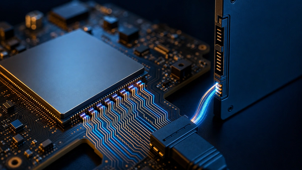
Industry update — AMD unveiled its second-generation Kintex UltraScale+ FPGA family, delivering up to 5x the memory bandwidth of the prior generation, PCIe Gen4 support, and guaranteed product availability through 2045 (AMD, February 2026).
Putting a real SATA SSD or hard drive behind a Kintex UltraScale+ device is a well-trodden path, but the bring-up trips up first-time integrators in predictable places: the transceiver has to speak SATA’s out-of-band handshake, the clocking has to be clean enough for a 6 Gb/s serial link, and the command layer has to present something your application logic can actually use. This guide walks the implementation of a SATA Host IP core — the FPGA driving the drive — on AMD’s Kintex UltraScale+ family, from the GT transceiver up to an optional file system, without any soft CPU in the datapath. In one sentence: you map the SATA link onto a single GTH or GTY transceiver, let the host core drive the out-of-band handshake, and expose block read and write over AXI to your application logic.
The short version
A SATA Host implementation on Kintex UltraScale+ maps cleanly onto the device’s GTH or GTY transceivers. You configure one GT lane for the SATA line rates (1.5 / 3 / 6 Gb/s), give it a clean reference clock, and let the host core drive the OOB signaling handshake that brings the link up. Above the PHY sit the link, transport and command layers, which expose a simple read/write interface — typically wrapped in AXI — to your application. Add an exFAT file-system core if you need named files on a drive a PC can also read. No processor, no operating system, deterministic timing.
Host vs device: which core you need
In every SATA link there is exactly one host and one device. The host issues commands; the device answers. Both roles can live in an FPGA, and they are separate IP cores with opposite jobs. This article is about the host role, where your Kintex UltraScale+ design behaves like the computer that reads and writes an attached SSD or HDD — the pattern behind recorders, data loggers and acquisition storage.
If instead you need the FPGA to appear as a drive to an external computer — drive emulation, a secure storage front-end, a bridge — that is the SATA Device role, and a different core. Getting this decision right first saves a great deal of rework; if you are unsure, our SATA Host and Device selection guide draws the line in detail. Everything below assumes you have settled on the host role.
What Kintex UltraScale+ brings to a SATA link
Kintex UltraScale+ is a strong fit for SATA because the interface leans almost entirely on one resource the family has in quantity: high-speed serial transceivers. The relevant public facts:
- GTH and GTY transceivers. Kintex UltraScale+ parts carry GTH transceivers, and higher-end members add GTY. Both comfortably cover the SATA line rates — SATA III tops out at 6 Gb/s, well inside their range — so a single lane carries the whole link.
- OOB-capable serial I/O. SATA’s link negotiation happens through out-of-band electrical-idle bursts rather than normal data. The transceivers expose the primitives needed to generate and detect those bursts, which is what makes a native SATA PHY possible without external glue.
- Ample fabric and block RAM. The link, transport and command layers are ordinary synchronous logic, and the block RAM handles Frame Information Structure (FIS) buffering and any queued commands. None of this stresses a mid-range UltraScale+ device.
Because the whole interface fits in a single transceiver quad plus a modest slice of fabric, you can usually add SATA storage to a Kintex UltraScale+ board you already selected for other reasons, rather than choosing the part around the drive. Targeting an Altera device instead of AMD? The equivalent path is covered in our Altera SATA Host IP support.
The implementation flow, step by step
The work divides into five stages, from the physical link upward. Each builds on the one before, so it pays to bring the link up cleanly before worrying about throughput.
1. Configure the transceiver (GT)
Start at the GT. You instantiate one lane (GTH or GTY, depending on your part) and set it for the SATA line rates you intend to support — usually all three of 1.5, 3 and 6 Gb/s so the link can negotiate down to whatever the drive accepts. The datapath width between the transceiver and the fabric is a design choice that trades clock frequency against bus width; the host core defines what it expects. SATA uses 8b/10b line coding, so either the transceiver’s built-in 8b/10b block or the core handles encoding and decoding.
2. Get the clocking right
A serial link is only as good as its reference clock. The GT’s PLL synthesizes the serial bit rate from an external reference clock (150 MHz is a common choice for SATA, but the core’s requirement governs), so that clock must be clean and low-jitter and routed on a dedicated clock-capable input. From the transceiver you derive the user-side clock domain in which the link, transport and command logic runs. Plan the clock-domain crossing between that recovered/user clock and your application clock early — it is a frequent source of late-stage bugs.
3. Bring up the PHY and the OOB handshake
This is the stage unique to SATA. Before any data flows, host and device exchange an out-of-band (OOB) signaling sequence to establish the link and negotiate speed. The host asserts a reset burst; the device answers; the two then wake the link and settle on the highest common line rate, stepping down from 6 Gb/s if needed. The host core drives this state machine and steers the transceiver’s OOB controls. When it completes, the PHY reports the link is up and locked at the agreed generation — the signal your application waits on before issuing commands.
4. Alignment and the link / transport layers
With the link up, the receiver aligns to the incoming symbol stream using SATA’s alignment primitives, and the link layer takes over: primitive handling, flow control, CRC and the framing of FIS structures. The transport layer assembles and disassembles those FIS frames into the register and data payloads the command layer works with. In a well-packaged core these layers are internal — you do not implement them — but understanding that they exist helps when you read status flags or debug a stalled transfer.
5. Command layer and AXI integration
At the top sits the command layer, which turns “read these blocks” and “write this buffer” into the correct FIS exchanges, including native command queuing where used. This is the surface your application touches. In an UltraScale+ system it is natural to wrap that surface in AXI: an AXI4 or AXI4-Stream data path for the payload and an AXI4-Lite channel for control and status, so the SATA host drops into a standard block design alongside your other IP. Your logic supplies a logical block address, a length and a buffer; the core handles the rest and raises a completion.
Interface signals and where the logic goes
Every SATA Host integration comes down to the same handful of signal groups. The table below is generic — exact port names and widths follow the specific core — but the shape holds across implementations.
| Signal group | Direction | Purpose |
|---|---|---|
| GT reference clock | In | Low-jitter clock feeding the transceiver PLL that synthesizes the SATA line rate. |
| Serial pair (TX+/TX−, RX+/RX−) | In/Out | The differential SATA link to the drive, routed from the GT to the connector. |
| User / link clock | Out | Clock domain in which the link, transport and command logic runs. |
| Command interface (AXI-Lite) | In | Issue read/write commands: logical block address, length, control. |
| Data interface (AXI / AXI-Stream) | In/Out | Payload movement to and from the drive. |
| Status / link-up | Out | Link state, negotiated generation, error and completion flags. |
On the resource side, the honest way to think about it is by category rather than a fixed count, because usage scales with your datapath width, buffering depth and feature set:
| Resource | Consumed by |
|---|---|
| Transceiver (GT) | One serial lane for the SATA link, plus its PLL. |
| Fabric logic | Link, transport and command state machines; OOB control; CRC. |
| Block RAM | FIS buffering and any queued-command / data FIFOs. |
| Clocking | Reference-clock input plus the derived user clock domain. |
For the actual utilization figures on your target part and configuration, ask the core vendor for the numbers against your exact device and datapath — they depend on choices only you make, so any single published figure would mislead.
Adding a file system: exFAT FS IP
A raw SATA Host core reads and writes logical block addresses — sectors, not files. For many recorders that is all you need: stream capture to a contiguous region and read it back by offset. But if the drive has to be removable and readable on a PC, or your application thinks in named files, you want a file system on top.
An exFAT file-system IP core layers that capability onto the SATA host without a processor. exFAT is the natural choice because it is the standard for large removable media and is mounted natively by Windows, macOS and Linux, so a drive your FPGA wrote drops straight into an analyst’s laptop. The file-system core sits between your application and the SATA host: your logic opens, writes and closes files; the core translates that into the block reads and writes the SATA host executes. It keeps the whole path in hardware, preserving the deterministic timing that made an FPGA storage design attractive in the first place.
Treat the file system as optional. If you control both the writing and the reading side and never remove the media, raw block access is simpler and leaner. Reach for exFAT specifically when interchange with general-purpose computers matters.
Bring-up and verification
A pragmatic order of operations shortens debug:
- Prove the reference clock and GT lock first. Nothing above the PHY can work until the transceiver is up on a stable clock. Confirm PLL lock before anything else.
- Watch the OOB sequence. Most first-time failures are here: no device response, or a link that negotiates to the wrong generation. The core’s status flags tell you where the handshake stopped.
- Do a single-block read, then write. Identify the drive and read one known sector before attempting streaming. A working single transfer proves the whole stack end to end.
- Then push throughput. Only once correctness holds do you scale to sustained streaming and confirm the drive keeps up without back-pressuring your capture.
Keep the negotiated line rate visible during bring-up. A link that silently drops from 6 Gb/s to 3 Gb/s — a cable, connector or signal-integrity issue — looks like a throughput bug much later if you were not watching the generation.
When this is the wrong approach
SATA on Kintex UltraScale+ is an excellent fit inside its envelope, but not everywhere:
- You need multiple gigabytes per second. After 8b/10b coding and protocol overhead, a SATA III link’s practical throughput sits well below its nominal 6 Gb/s. When you truly need more, an NVMe Host core over PCIe on the same UltraScale+ transceivers is the right move — we weigh the two in SATA vs NVMe for FPGA storage.
- You store only tiny amounts. For configuration or calibration data, QSPI flash is far cheaper in logic than a full storage controller.
- The role is actually “device”. If the FPGA must present itself as a drive to a host, you need the SATA Device core, not the host implementation described here.
Need a SATA host or device IP core for a specific FPGA family? Talk to the team that builds them.
Frequently asked questions
What is a SATA Host IP core?
A SATA Host IP core is a block of FPGA logic that implements the host side of the Serial ATA protocol — the PHY on a GTH or GTY transceiver, plus the link, transport and command layers — so the FPGA can read and write an attached SSD or hard drive. On Kintex UltraScale+ it runs with no CPU and presents a block read/write interface, usually wrapped in AXI.
Does a SATA Host core on Kintex UltraScale+ need a processor?
No. The link, transport and command layers are implemented entirely in FPGA logic on the GTH/GTY transceivers, so the host runs with no CPU, no operating system and deterministic timing. You issue block commands directly from your application logic, typically over AXI.
Which transceivers does SATA use on Kintex UltraScale+?
The GTH transceivers present across the family, and the GTY transceivers on higher-end parts. A single lane covers SATA’s 1.5, 3 and 6 Gb/s line rates, and the transceiver’s out-of-band signaling support is what enables a native SATA PHY.
Why is OOB signaling important in a SATA implementation?
SATA brings the link up through an out-of-band handshake — electrical-idle bursts exchanged before any data — that resets the link and negotiates the line rate. If the transceiver and host core do not drive this sequence correctly, the link never comes up, which is why OOB is the most common bring-up sticking point.
How do I connect a SATA host to the rest of my design?
Most integrations wrap the command layer in AXI: an AXI4 or AXI4-Stream path for data and AXI4-Lite for control and status. That lets the SATA host sit in a standard block design next to your other IP, receiving a logical block address, a length and a buffer, and returning a completion.
Can I store named files instead of raw sectors?
Yes, by adding an exFAT file-system IP core above the SATA host. It translates file operations into the block reads and writes the host executes, keeping everything in hardware. exFAT is chosen so the media is readable on Windows, macOS and Linux without extra software.
When should I use NVMe instead of SATA on UltraScale+?
When your sustained throughput needs to exceed what a SATA III link delivers once 8b/10b coding and protocol overhead are counted. An NVMe Host core over PCIe uses more logic but reaches multiple gigabytes per second on the same UltraScale+ transceivers.
Need a SATA Host core targeted at a specific Kintex UltraScale+ part, or want the utilization figures for your exact device and datapath? A short technical exchange usually settles it.
- SATA-IO — Serial ATA ecosystem and generations overview
- SATA-IO — Serial ATA specification (OOB signaling, link/transport layers)
- AMD — UltraScale Architecture GTH Transceivers User Guide (UG578)
- AMD — UltraScale Architecture GTY Transceivers documentation
- AMD — Kintex UltraScale+ FPGA family overview