
The EF4442 ARINC 429 receiver has reached end of life: it is no longer sold, yet boards built around it can still have years of service ahead. One way to keep them in service is to rebuild the receiver function inside a small FPGA with the MEF4442A ARINC 429 IP from Logic Design Solutions. This guide explains what the MEF4442A takes over, where it differs from the original part, and what the migration involves for your board and your software.
The short answer
When the EF4442 can no longer be bought, the receiver function can move into an FPGA. The MEF4442A is a VHDL macro based on the EF4442 in mode A: 4 independent receivers, 1 transmitter and a simple 8-bit CPU interface. It covers mode A only, and its product brief states that it is not strictly compatible with the EF4442. Treat the replacement as a short design project: compare the register map and software behaviour, assign the pinout in the FPGA, rerun the delivered VHDL testbench, then requalify according to your programme. Logic Design Solutions can customise the macro and integrate other functions in the same FPGA.
EF4442 end of life: where things stand
The EF4442 is a 4-channel ARINC 429 receiver. It has two operating modes. In mode A, it provides 4 receivers and 1 transmitter on an 8-bit data bus, with a direct interface to a 6800-family microprocessor. In mode B, its parameters are fixed by hardware.
The part is no longer sold. For a programme that still has boards to build or repair, that leaves three routes: find remaining inventory, redesign the board around a different controller, or keep the board architecture and replace only the receiver function. The third route is what an FPGA IP is for. It is often the least disruptive option when the surrounding hardware, the software and the qualification file are already in place.
The protocol on the bus does not change with the replacement. If you need a refresher on ARINC 429 word format, labels and data rates, see our ARINC 429 protocol guide; we will not repeat it here.
What the MEF4442A takes over
The MEF4442A is an ARINC 429 synchronous multichannel receiver and transmitter, written in VHDL. Its product brief (version 1.3) lists the following functions.
| Function | MEF4442A |
|---|---|
| Reference behaviour | EF4442 in mode A |
| Channels | 4 independent receivers, 1 independent transmitter |
| CPU interface | Simple CPU interface, 8-bit data bus (chip select, read/write, 8 data bits, 2 address bits, interrupt request) |
| ARINC 429 line interface | “1” and “0” lines, RZ code |
| Labels and parity | Label control by software; odd parity or no parity |
| Other | Interrupt output, test mode |
| Clock | Operating frequency depends on the speed grade of the target FPGA |
Because the macro follows the EF4442 in mode A, the review of your existing driver starts from a familiar model: the same channel count and an 8-bit processor bus.
Mode A only, and “not strictly compatible”
Two limits matter before anything else, and we prefer to state them up front.
- Mode A only. The MEF4442A is based on the EF4442 in mode A. A board that uses the EF4442 in mode B, with its parameters fixed by hardware, needs a closer look: the MEF4442A does not reproduce mode B, so the settings fixed by hardware on the original part have to be reviewed with Logic Design Solutions, which can customise the macro.
- Not strictly compatible. These are the product brief’s own words. The ARINC 429 receiver function is taken over, but the FPGA is not a pin-for-pin substitute for the EF4442, and the macro’s behaviour has to be checked against what your software relies on.
In practice, the differences sit in the package (a new device with its own footprint, supplies and pin assignment), in the register map and timing seen by the software, and in the qualification file, since a new device on the board calls for new verification. The IP can shorten that work; it does not remove it. Saying so early saves a programme from discovering the gap during integration.
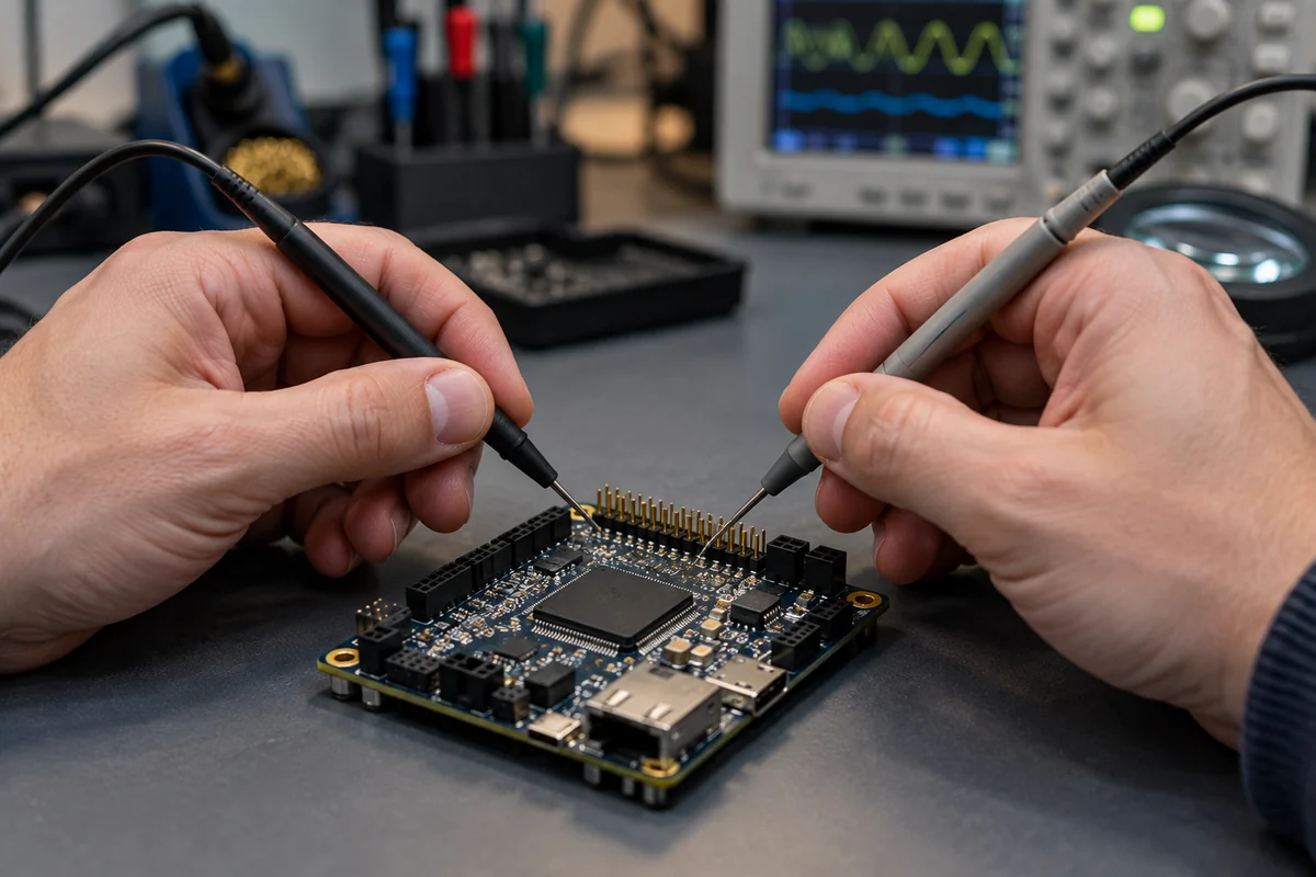
EF4442 replacement: the migration, step by step
An EF4442 replacement with the MEF4442A follows four steps, each feeding the next.
- Compare the register map and the software behaviour. Take the driver your board runs today and check each access against the MEF4442A datasheet: register addresses, bit fields, label programming, parity settings, interrupt handling. List every difference and decide whether the software changes or the macro does.
- Assign the pinout in the FPGA. Map the CPU bus, the interrupt line and the ARINC 429 “1” and “0” lines to FPGA pins that suit your board layout. The product brief counts 26 I/Os if every signal of the macro is brought out of the device.
- Rerun the delivered testbench. The macro ships with a VHDL testbench for behavioural and post-layout (gate-level) simulation. Run it on your configuration, after any customisation, before the device goes on a board.
- Requalify according to your programme. Simulation results are evidence for the receiver; system-level acceptance remains defined by your programme’s own rules, on the real board with real traffic.
Logic Design Solutions can take on part of this work, from customising the macro to integrating it with other functions in the same device.
A small flash FPGA as the new home
In our view, a small flash FPGA is a sensible host for the MEF4442A, for example a device from the Microchip IGLOO family. Flash FPGAs are non-volatile, so they start up without an external configuration memory. IGLOO devices are low-power 130 nm parts.
The occupancy figures published in the MEF4442A product brief date from 2003 and cover the Actel families of that time:
- Actel 54SX-A: 1,300 modules;
- Actel ProASIC+: 1,900 core cells;
- Actel Axcelerator: 600 flip-flops and 1,100 combinatorial cells.
Actel is now part of Microchip. We have not published a measured occupancy on IGLOO, so the right device for your board is something we size with you from your configuration rather than a figure we would quote here. Logic Design Solutions can size the FPGA’s density and I/O count to your specification.
What Logic Design Solutions delivers
The MEF4442A is purchased under a licence agreement. The delivery includes:
- the VHDL source code of the macro;
- a VHDL testbench for behavioural and post-layout (gate-level) simulation;
- the datasheet;
- a user guide covering simulation, synthesis and place and route;
- a constraint file.
A bitstream with its datasheet is available as an option. Six months of email and phone support by Logic Design Solutions are included with the macro; that support does not cover modifications made by the user, and maintenance contracts are available beyond it. Because the VHDL source is delivered, the receiver function is no longer tied to one purchased chip, which is precisely the dependency a discontinued part exposes.
Logic Design Solutions can also integrate the macro with other pre-designed functions in the same FPGA. On an ageing board, that can be a chance to absorb a second obsolete part or some surrounding logic into the same device.
When four channels are not enough
If the board needs more than 4 receive channels or more than 1 transmitter, look at the M68C429A. It is an enhanced version of the EF4442, based on the TS68C429A: 8 receivers, 3 transmitters with FIFO, a 68000-type CPU interface on a 16-bit data bus, and data rates up to 2.5 Mbit/s. Like the MEF4442A, it is delivered as VHDL source and is not strictly compatible with the part it is based on. Our guide to replacing the TS68C429A at end of life with the M68C429A covers it in detail.
For a new design with no legacy register map to preserve, a replacement macro is not the right starting point. Our current ARINC 429 IP is built for that case, and our article on the ARINC 429 IP core for FPGA explains how it fits a modern design. For a recording application, see designing avionics data recorders on FPGA with ARINC 429 IP. If you are still choosing a bus, see our comparison of ARINC 429, ARINC 629 and MIL-STD-1553.
In summary
The EF4442 is no longer sold, but the receiver function it provided can live on in a small flash FPGA. The MEF4442A is based on the EF4442 in mode A, with 4 receivers, 1 transmitter and an 8-bit CPU interface, delivered as VHDL source with its testbench. It covers mode A only and is not strictly compatible with the original part: plan for a register and software review, a pinout in the FPGA, a testbench run and a requalification. When 4 channels are not enough, the M68C429A is the next step.
How we wrote this article
The MEF4442A and M68C429A facts come from the Logic Design Solutions product briefs, version 1.3. The EF4442 description and its availability status are Logic Design Solutions’ own statement; we give no discontinuation date because we have found no dated notice to cite. The occupancy figures are the ones published in the 2003 brief, on Actel devices; they have not been re-measured on current FPGA families. Where we give a recommendation, it is our opinion, and we write it as such.
This article gives technical criteria and our point of view. It does not replace a review of your own board and programme requirements.
It is published by Logic Design Solutions, which therefore has an interest in the subject.
Sources
- Logic Design Solutions, MEF4442A Product Brief, version 1.3, January 2003, and MEF4442A product page.
- Logic Design Solutions, M68C429A Product Brief, version 1.3, January 2004, and M68C429A product page.
- Microchip, IGLOO Low Power Flash FPGAs with Flash*Freeze Technology, datasheet.