Features
– 1 Independent Receivers (Rx) with FIFO
– 1 Independent Transmitter (Tx) with FIFO
– Decoding signals interface type
– 16-Bit Data-bus
– Direct addressing of all Registers
– ARINC 429 Interface : ‘1’ and ‘0’ Lines, RZ code
– Support all ARINC 429 Data Rate Transfer and up to 2.5 Mbit/s
– Multi Label Capability
– Parity Control : Odd, Even, No Parity, Interrupt Capability
– Independent Interrupt Request Line for Rx and Tx Functions
– FPGA speed grade operating frequency dependant : system clock up to 70 MHz
– Available in VHDL source code format for ease of customization
– DO254 design, verification and traceability documentation available on request
– Can be customized by Logic Design Solutions
General Description
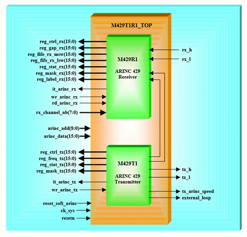
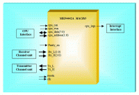
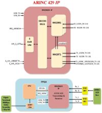
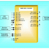
The M429T1R1 macro implements a synchronous single-chip ARINC 429 Transmit and Receive Controller Macro capable of linking one CPU to one ARINC 429 bus. The macro controls all ARINC 429 bus specific sequences, protocol and timing. The M429T1R1 macro interface allows the parallel-bus microprocessor to communicate bidirectionally with the ARINC 429 bus. This macro can be customized according to specific needs (application-specific requirement). Any other pre-designed functions can be integrated into the FPGA. FPGA density and I/O requirements can be defined according to customer specification.

