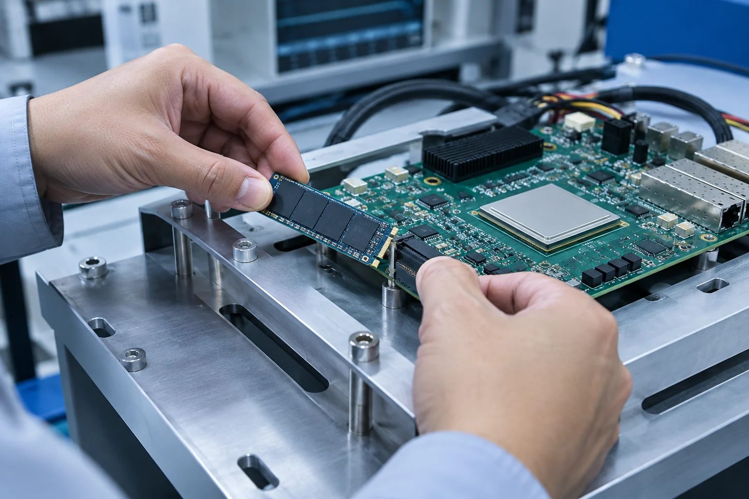
“Space-grade NVMe” does not, on its own, establish that an SSD or FPGA host-IP design is suitable for a mission. The review question is whether the radiation evidence supports the specific component and design claim being made.
The short answer
Space-grade NVMe suitability for an FPGA design depends on mission-specific evidence, not the label alone.
We recommend defining the radiation environment and mission requirements, then keeping evidence separate for the SSD assembly, test fixture, and FPGA host IP.
Radiation results for a tested assembly support conclusions only within the tested configuration, exposures, and operating modes, but they do not automatically establish readiness of a distinct FPGA host-IP design.
Record unsupported items as unresolved, and reserve an IP-readiness conclusion for evidence that directly addresses the IP.
What does “space-grade NVMe” mean for an FPGA design?
For an FPGA design, “space-grade NVMe” is a mission-specific assurance question, not a universal qualification; assess it against the requirements and evidence for the specific drive and system.
Our analysis starts with mission assumptions. NASA’s description of radiation-hardness assurance covers defining the environment, selecting and testing parts, spacecraft layout, radiation-tolerant design, and mission, system, and subsystem requirements; it also describes organizing this work by activity or examining it at different levels of scope.
Start with mission assumptions. Use the activities in NASA’s radiation-hardness assurance process as review fields: record the defined environment, parts selection and testing, layout considerations, radiation-tolerant design, and applicable requirements. Keep each item tied to its scope, whether mission, system, or subsystem.
For each item, identify whether the evidence applies to the NVMe drive, the system, or the FPGA IP, and note any open assumptions. Keep the drive decision separate from the FPGA IP decision. Document requirements and evidence for each; mark unsupported review items as unresolved instead of treating the product label as an assurance case.
The NASA SSD study describes commercially available drives that were not otherwise hardened for a radiation environment and test samples that were not specially prepared. That description applies to the drives and samples in the study; it does not establish whether a different SSD meets a particular mission’s requirements.
Keep the assurance claim tied to the specific evidence and scope. The review record should distinguish documented evidence from open decisions, including what applies to the drive and what applies to the FPGA IP.
What can radiation tests establish about SSD assemblies used with NVMe test fixtures?
Radiation tests establish how a specific SSD assembly responds to defined exposures and operating modes; for an NVMe test fixture, apply each result only within the conditions covered by the test, as described in the study’s assembly-level assessment.
The study assessed automotive- and industrial-grade SSD assemblies for total ionizing dose (TID) and single-event effects (SEE) across multiple operating modes. It used three exposure types at three facilities, according to the study’s description of its assembly-level tests:
| Exposure | Facility reported in the study |
|---|---|
| High-energy heavy-ion beams | NASA Space Radiation Laboratory (NSRL) |
| 200 MeV protons | Massachusetts General Hospital’s Francis H. Burr Proton Therapy Center (MGH) |
| 1 MeV gamma rays | NASA Goddard Space Flight Center’s Radiation Effects Facility (GSFC REF) |
Assembly-level testing assesses the SSD within a system, while component-only testing considers individual parts. For a fixture assessment, assembly-level results are more relevant than component-only results, as the study’s comparison of parts tested within a system and separately illustrates.
The study reports that parts were tested. It also reports that SSD assemblies were tested for SEE response. These findings are detailed in the paper’s discussion of SSD radiation-assurance concerns.
TID and SEE support different conclusions. The paper says the tested SSDs may have acceptable TID performance in the lowest dose environments or when heavily shielded, while raising concerns about their SEE performance from a testing standpoint, in its reported assessment. That distinction matters.
For an NVMe test fixture, our recommendation is to reproduce the complete intended test case, rather than test only the most common or most concerning application. A result from one operating mode should not be treated as evidence for modes the test did not cover.
How do active radiation tests handle drive-level failures?
Active radiation tests classify SSD timeouts by recovery: a drive is recoverable if an automatic power cycle restores it, and unrecoverable only if the cycle fails and all manual recovery attempts fail, under the study’s recovery criteria.
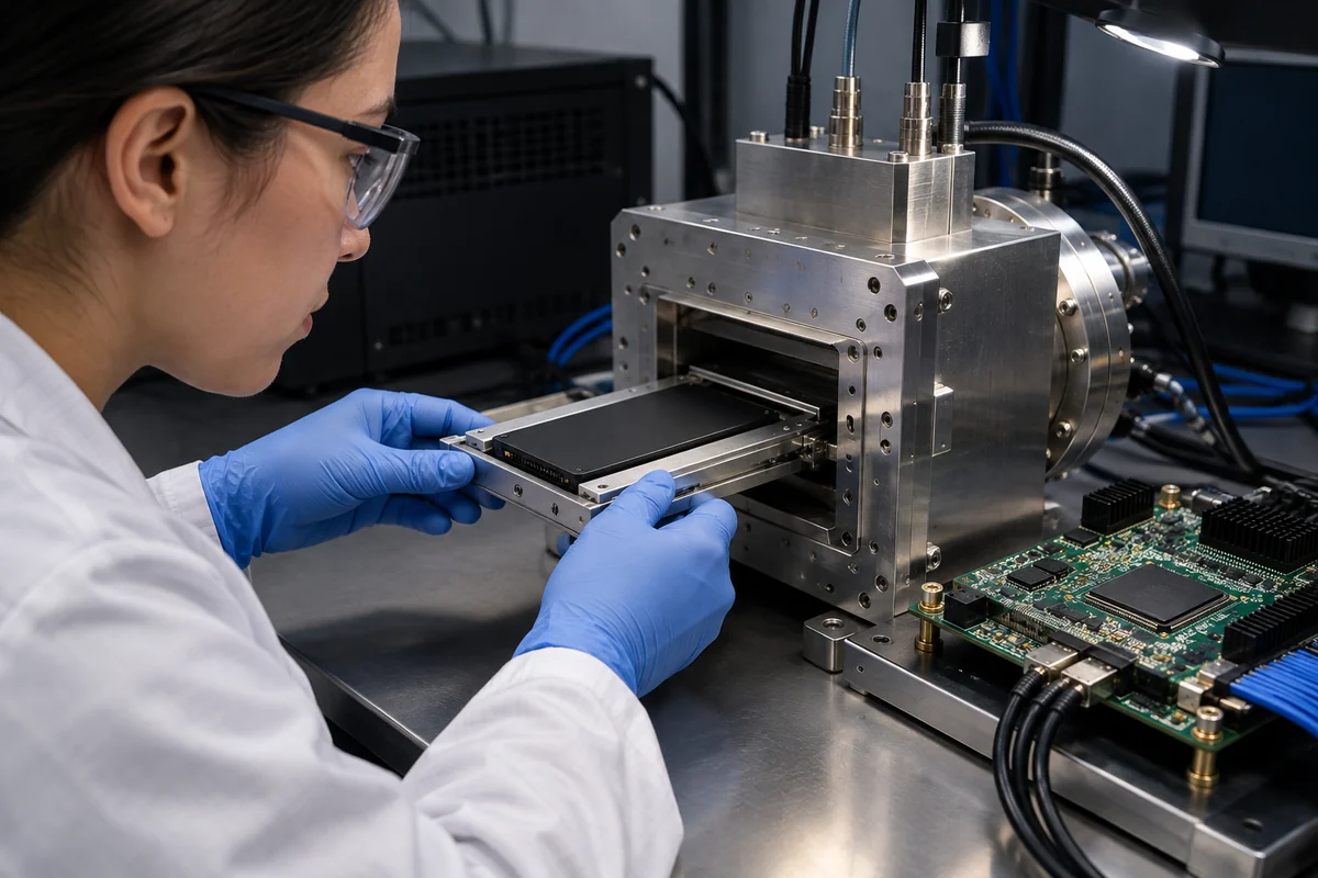
The NASA test arrangement isolated the SSD in the beam with passive NVMe extenders. It also used a digital I/O module connected to the test computer to provide inhibit signals for facility beam delivery and power while recovery was attempted, according to the NASA test arrangement.
A timeout alone is not the classification. The active-testing study distinguishes the timeout from the drive’s recovery outcome.
| Outcome | Classification criterion |
|---|---|
| Recoverable | An automatic power cycle restores the drive, under the study’s recovery criteria. |
| Unrecoverable | The automatic power cycle does not restore the drive, and all manual recovery attempts fail, under the study’s recovery criteria. |
The recovery outcome, not the timeout alone, sets the classification, according to the active-testing study. For an FPGA-side test record, keep the read or write timeout separate from the automatic power-cycle result. If the cycle does not restore the drive, record whether all manual recovery attempts failed.
Our recommendation is to preserve that sequence in the test record: note the timeout, record the automatic power-cycle result, then capture the outcome of manual recovery if needed. Keep the symptom and recovery outcome in separate fields.
Sources
- NASA NTRS record describing the SSD test setup
- NEPP paper describing active testing and recovery classifications
What remains unresolved when assembly-level SSD tests inform host-IP readiness?
Assembly-level SSD tests do not establish FPGA host-IP readiness. They support conclusions about the tested SSD assembly and fixture, not a separate host-IP claim, as the study’s setup and stated limits show.
The fixture used passive PCIe extenders with standard M.2 SSD slots and PCIe-to-USB adapters, keeping the NVMe-to-USB microcircuits well clear of the beam, according to the test setup description. The data-processing computer could sit at the far end of a USB-C cable, with peak data rate traded away, according to the fixture description. That boundary matters: the tested SSD assembly is not the same claim as host-IP readiness.
The study notes that off-the-shelf SSDs may offer little customization, limited error reporting, and potentially no architectural details. It also reports that all parts tested failed unrecoverably, for reasons likely more related to architecture than to a familiar single-event latchup signature, according to the study’s discussion of screening limits. For an FPGA team, limited device visibility is a reason to keep conclusions tightly scoped, not to extend an assembly result to a separate design claim.
Our recommendation is to label each conclusion by the object it supports: the SSD assembly, the fixture path, or the FPGA host IP. Keep the test setup and its stated limitations beside the conclusion. That makes the boundary between assembly-level evidence and the IP-readiness claim explicit.
Keep each conclusion tied to its evidence.
- State whether the cited result concerns the SSD assembly or the FPGA host IP.
- Record which supporting components were kept out of the beam and how the fixture connected the drive.
- Keep any host-IP readiness claim separate unless the cited evidence directly addresses that claim.
Use precise wording in the review record: the SSD assembly was tested using the stated fixture. Reserve “host IP is ready” for evidence that directly supports the IP-level conclusion.
What does an embedded eMMC example show about ECC placement?
According to the embedded eMMC module example, ECC is assigned to the module’s integrated controller. The example does not show how FPGA NVMe IP handles ECC.
The source describes an eMMC 5.1 module whose integrated controller handles wear leveling, bad block management, and error correction (ECC), “ensuring long-term data integrity and simplified system integration.” Read the description of the module’s integrated controller. The architectural point is specific: ECC is assigned to the eMMC module’s integrated controller in this example. The source’s account of the controller’s responsibilities does not assign ECC to FPGA logic or specify how an FPGA NVMe implementation handles it.
For a design review, keep the example’s scope attached to the claim. Label the component, state the responsibility attributed to it, and identify the supporting documentation. This helps keep an eMMC statement from being carried into an FPGA NVMe block diagram as though it described the same implementation.
Our recommendation is to avoid transferring the eMMC controller’s ECC assignment to FPGA NVMe IP, because the source describes a module-level responsibility and does not establish how a target FPGA design handles ECC. In specifications and review notes, use precise wording: “the cited eMMC module’s integrated controller handles ECC” is supported; “the FPGA NVMe IP handles ECC” is not established by this example.
When documenting a design, separate the questions:
- Which component does the statement describe?
- Which responsibilities does the source explicitly assign to that component?
- Does the claim concern the eMMC module or the FPGA NVMe IP?
Keep unsupported details out of the answer. The source does not describe an FPGA implementation, define an ECC algorithm, or state how responsibilities are divided between an NVMe host and storage hardware. Name the block, then state only the responsibilities supported for it; that keeps the comparison useful without turning one module description into a claim about another design.
When is a SATA host path a better fit than an NVMe host path?
A SATA host path is a better fit when embedded, space-limited, or low-power storage matters and the workload fits SATA’s stated link rates; the cited comparison favors PCIe 3×4 M.2 for continuous processing or heavy computing.
Start with workload.
The SATA-IO ecosystem page lists transfer rates of 6.0, 3.0, and 1.5 Gb/s, so use those figures as a first sizing check, not as a claim about the rate a particular FPGA implementation will sustain.
Our recommendation: favor SATA when its link-rate options fit the storage requirement and embedded or low-power positioning matters. Treat physical fit and workload fit as separate design questions; the comparison distinguishes the interfaces by use case. For continuous processing or heavy computing, the comparison points toward PCIe 3×4 M.2.
Keep the evidence boundary clear. The comparison of M.2 SSD use cases and the SATA-IO ecosystem page do not establish whether a particular NVMe host IP is suitable for a space-grade design.
Sources
Frequently asked questions
What is NVMe space?
For an FPGA design, we treat “space-grade NVMe” as a mission-specific assurance question, not a label that proves a drive is suitable. The review should tie evidence about the environment, drive testing, system layout and radiation-tolerant design to the relevant mission, system or part scope.
Which type of NVMe SSD is best?
There is no single best type for every FPGA mission. We recommend choosing based on the mission requirements and evidence for the specific drive and operating modes. Keep test results tied to what was tested, and assess the SSD assembly separately from FPGA host-IP readiness.
In summary
Now make the review record distinguish the SSD assembly, fixture path, and FPGA host IP, and attach each conclusion only to evidence that addresses that object. Mark unsupported items unresolved, and keep host-IP readiness open unless the evidence directly addresses the IP. Then decide whether the workload and interface requirements point to a SATA host path or an NVMe host path.
How we wrote this article
The sources we consulted are listed at the end of the article, consulted on 2 October 2026. Where we cite none, it is our opinion, and we write it as such.
Sector figures come from notre analyse de la base SIRENE de l’INSEE, stock au 1er août 2026. They count establishments; they measure neither output nor sales.
This article gives buying criteria and our point of view. It does not replace a professional’s advice on a specific situation.
It is published by Logic Design Solutions, which therefore has an interest in the subject.
Sources
- Solid State Drive Radiation Assurance With Active Testing, nepp.nasa.gov
- Solid State Drive Radiation Assurance With Active Testing – NASA Technical Reports Server (NTRS), ntrs.nasa.gov
- Teledyne HiRel Semiconductors Launches eMMC 5.1 Module : EEJournal, eejournal.com
- Industrial M.2 solutions for AIoT applications …, eenewseurope.com
- Avionics Radiation-Hardness Assurance for Safe Exploration Beyond Low Earth Orbit – NASA, nasa.gov
- The SATA Ecosystem | SATA-IO, sata-io.org