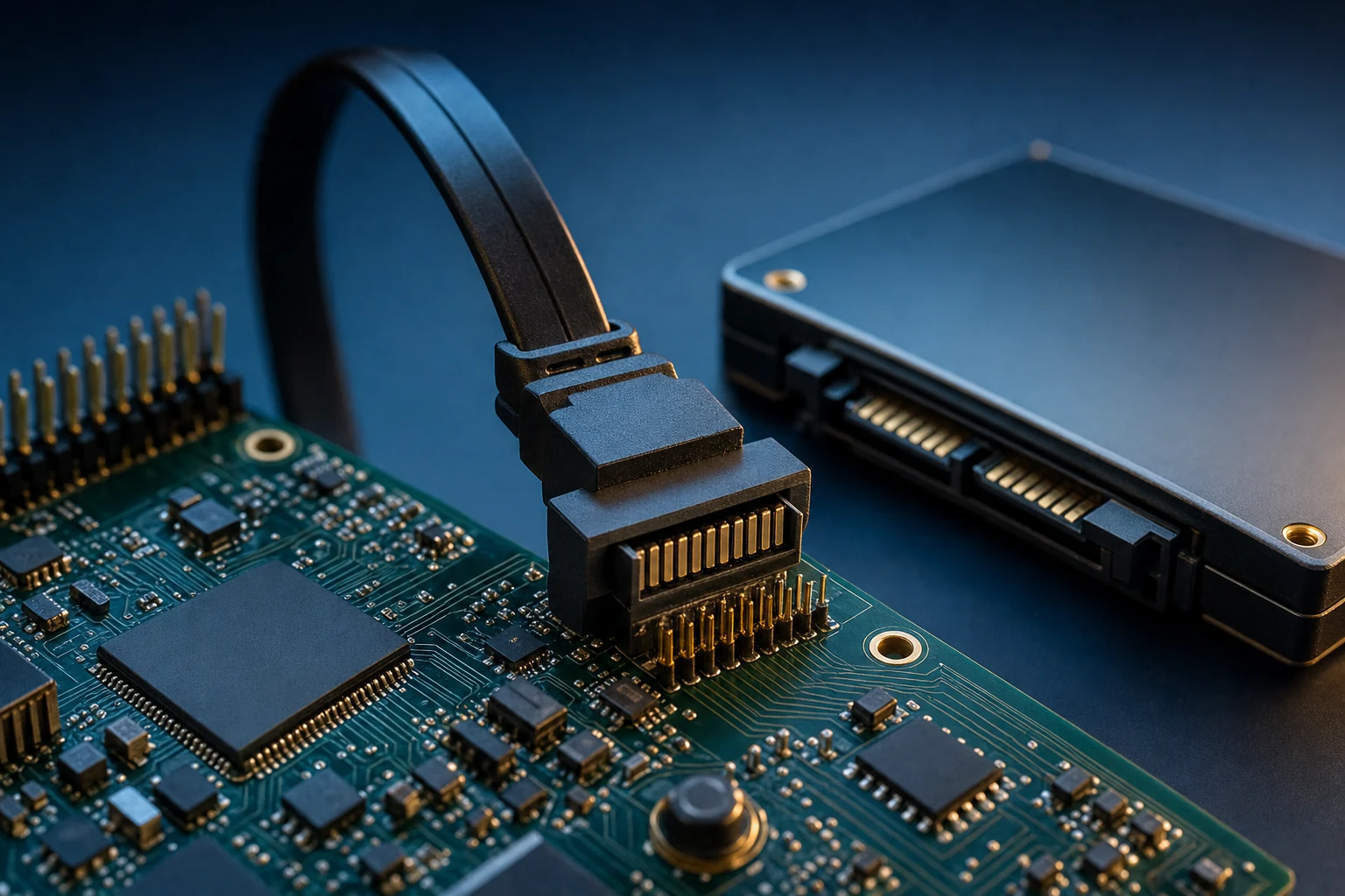
Industry update — The combined revenue of the top five NAND flash brands rose 77 % quarter-on-quarter to US$68.87 billion in Q2 2026, with steady AI-server demand for enterprise SSDs producing a supply shortage across the NAND market (TrendForce, 18 August 2026). When drives get scarce and expensive, the interface a design is built against decides which drives it can still qualify — which makes knowing exactly what the SATA protocol does, and where it stops, a procurement question as much as an engineering one.
In short: SATA is a four-layer serial protocol — PHY, link, transport and (device side only) command. Everything an FPGA engineer needs to reason about lives in those layers: OOB wake-up bursts, 8b/10b encoding, scrambling and CRC, and Frame Information Structures (FIS) carrying ATA commands and data at 1.5, 3 or 6 Gbit/s.
SATA is often called “the simple one” next to PCIe and NVMe, and for an FPGA design that is largely true: one differential pair each way, one device per link, a command set inherited from ATA. But simple is not the same as obvious. Whether you are implementing a controller in fabric or evaluating a core someone else wrote, you need a working model of what the protocol does between the transceiver pins and your application logic — because that is where its cost hides: the out-of-band wake-up sequence, the primitives that keep a FIFO from overflowing, the FIS your transport layer builds and parses, and the queue depth that caps how much work a drive can hold at once. This page is that model, written for the person who has to close timing on it.
- The short answer
- The layer stack, and which layers land in your fabric
- Speeds, 8b/10b, and the clock that falls out of them
- OOB signalling: how a SATA link wakes up
- The link layer: scrambling, CRC and primitives
- FIS types: the packets everything travels in
- ATA commands, NCQ and the 32-command ceiling
- Power states: Partial, Slumber, DevSleep
- Implementing or licensing: what actually changes
- Where this page stops
- Frequently asked questions
The short answer
The SATA protocol is a layered serial interface. The PHY layer handles the serial link itself: out-of-band (OOB) bursts to bring the link up and negotiate speed, 8b/10b encoding in the FPGA transceiver, comma detection, and conversion to a parallel word. The link layer frames that word stream: scrambling, CRC-32, and flow-control primitives that stop either side’s FIFO from over- or under-running. The transport layer builds and parses Frame Information Structures (FIS) — the packets that carry ATA task-file registers and payload. A command layer sits on top, but only on the device side; a host controller exposes the task file to your logic instead. Signalling runs at 1.5, 3 or 6 Gbit/s, which after 8b/10b overhead gives roughly 150, 300 and 600 MB/s of usable bandwidth.
The layer stack, and which layers land in your fabric
A SATA host controller implements PHY, link and transport. A SATA device controller implements those three plus a command layer, because a device has to interpret ATA commands and behave like a drive. That single asymmetry explains most of the size difference between host and device IP.
Vendor datasheets assume you already know that split. Our own SATA Host cores are documented as incorporating “the Transport layer, the Link layer and the PHY layer”; the SATA Device cores add “the Command Layer” on top of those three. Nothing else in the stack changes — the wire, the primitives and the FIS formats are identical in both directions.
- PHY layer. Serialisation, OOB detection, comma alignment, 8b/10b coding. On an AMD or Altera FPGA most of this sits in the hard transceiver (a GTH, GTX or equivalent), with the surrounding state machine in fabric. A core targeting AMD UltraScale+ GTHE4 transceivers, for example, detects OOB and COMWAKE, detects the
K28.5comma character and presents a 32-bit parallel output, and leaves 8b/10b encoding and decoding to the GTHE4 itself. - Link layer. Turns that word stream into frames: scrambling and descrambling, CRC-32 calculation and checking, primitive insertion and removal, BIST loopback modes, and power-state management shared with the PHY.
- Transport layer. Assembles and disassembles FIS, holds the shadow registers and the SATA SuperSet registers, handles 48-bit sector addressing, PIO and DMA transfer modes, and error-FIS retry.
- Command layer (device side). Decodes the ATA command in a received Register FIS, drives the media or buffer behind it, and produces the right response FIS. This is what makes an FPGA look like an SSD to a host.
The consequence for integration: your application logic never sees the wire. It sees a task file and a DMA or FIFO port; everything below is the core’s problem.
Speeds, 8b/10b, and the clock that falls out of them
SATA defines three signalling rates: 1.5, 3.0 and 6.0 Gbit/s. Because the line code is 8b/10b, 20 % of the raw bits are encoding overhead, so the uncoded rates are 1.2, 2.4 and 4.8 Gbit/s — that is, about 150, 300 and 600 MB/s. Those numbers are the ceiling of the link, before any protocol, file-system or media limit.
There is a second consequence that catches people out at timing closure: the system clock of a SATA controller is not a free parameter. If the link layer hands the transport layer a 32-bit word, the fabric clock has to carry the full uncoded rate. At 6 Gbit/s that is 4.8 Gbit/s ÷ 32 bits = 150 MHz. Halve the line rate and you halve the clock.
| Specification (SATA-IO naming) | Common shorthand | Signalling rate | Uncoded rate after 8b/10b | Practical ceiling | Clock_sys on a 32-bit LDS core |
|---|---|---|---|---|---|
| Serial ATA Revision 1.0 | SATA 1.5Gb/s (“SATA I”) | 1.5 Gbit/s | 1.2 Gbit/s | ~150 MB/s | 37.5 MHz |
| Serial ATA Revision 2.0 | SATA 3Gb/s (“SATA II”) | 3.0 Gbit/s | 2.4 Gbit/s | ~300 MB/s | 75 MHz |
| Serial ATA Revision 3.0 | SATA 6Gb/s (“SATA III”) | 6.0 Gbit/s | 4.8 Gbit/s | ~600 MB/s | 150 MHz |
One naming caveat that saves arguments in requirement documents: SATA-IO’s own guidance asks the industry not to use “SATA II” or “SATA III” — “SATA II” was the name of the committee, not a data rate, and “Gen 2” and “Gen 3” are internal specification conventions rather than product names. The recommended terms are “SATA 3Gb/s” and “SATA 6Gb/s”. The shorthand is unavoidable in conversation, and it appears in our datasheets and everyone else’s — but when a number goes into a specification, write the signalling rate, not the generation.
OOB signalling: how a SATA link wakes up
Before any data can flow, host and device negotiate through out-of-band (OOB) signalling: bursts of activity separated by defined idle gaps, detected by the transceiver rather than decoded as data. The host drives COMRESET, the device answers with COMINIT, a COMWAKE exchange brings both PHYs up, and the two ends then settle on the highest speed both support.
OOB matters to an FPGA engineer for one blunt reason: a generic SerDes is not enough. The transceiver has to generate and detect these burst patterns, and the surrounding state machine has to sequence them with the right timing. That is why SATA IP is always named against a specific transceiver primitive — GTHE4, GTH, GTX or an Altera equivalent — rather than against “an FPGA”.
Two practical notes. OOB is stable across generations: SATA-IO’s migration guidance states that Revision 3.0 uses the same frequency and signal type for OOB as Revision 2.6, which is why moving a design from 3Gb/s to 6Gb/s did not force teams to redesign their OOB circuitry. And the same COMRESET and COMINIT sequences are what a host controller uses to notice that a drive has been inserted or removed — hot-plug detection is not a separate mechanism, it is OOB seen from another angle.
The link layer: scrambling, CRC and primitives
The link layer wraps payload into frames and protects them: it scrambles transmit data (and descrambles receive data) to spread the spectrum, computes and checks a CRC-32 over each frame, and inserts control primitives — single reserved words that carry link state rather than data.
Two primitives deserve attention because they show up directly in FPGA symptoms:
- HOLD is the flow-control primitive. A controller inserts it automatically when its FIFO is about to overflow or underrun, which is how a SATA link tolerates a receiver that momentarily cannot keep up. If your application logic stalls, the link does not break — it fills with HOLDs and throughput quietly drops. That is the signature to look for when a benchmark lands below the link ceiling.
- CONT compresses repeated primitives on the wire, so a long idle or hold period is not transmitted as thousands of identical words. A link layer has to manage CONT in both directions; a decoder that ignores it will misread the bus in simulation.
BIST loopback and pattern-generation modes live here too — how you prove a channel electrically before trusting it with data, and the reason a BIST Activate FIS exists in the table below.
FIS types: the packets everything travels in
A Frame Information Structure (FIS) is the unit of transfer above the link layer: every command, status update and block of payload crosses the link inside one. Eight FIS types cover essentially all traffic, and a controller’s job is to build the ones it sends and route the ones it receives.
| FIS type | Direction | What it carries |
|---|---|---|
| Register FIS — Host to Device | Host → device | The ATA task-file registers: the command opcode, the LBA, the sector count. This is the “go” packet. |
| Register FIS — Device to Host | Device → host | Status and error registers plus the task file. Also the signature FIS the device sends after reset, which tells the host what kind of device it is. |
| Data FIS | Both | The payload itself. Everything else in this table exists to schedule these. |
| PIO Setup FIS | Device → host | Sets up a programmed-I/O transfer: direction, byte count, and the register state to apply at the end. |
| DMA Setup FIS | Device → host | Sets up a first-party DMA transfer — the mechanism behind queued (NCQ) commands. |
| DMA Activate FIS | Device → host | Tells the host it may now send its Data FIS. The device controls when write data arrives. |
| Set Device Bits FIS | Device → host | An asynchronous status update; for NCQ, this is how the device signals which queued commands have completed. |
| BIST Activate FIS | Both | Puts the link into a built-in self-test mode such as far-end loopback. Test path, not data path. |
AHCI — the register-level interface most software drivers expect — formalises this with a Received FIS Structure in host memory: dedicated slots for the DMA Setup, PIO Setup, D2H Register and Set Device Bits FIS, plus a 64-byte area for any FIS the controller does not recognise. Writing a bare-metal driver against a host core, that is the shape your receive handler should mirror even when you are not implementing full AHCI.
ATA commands, NCQ and the 32-command ceiling
SATA transports the ATA command set, which is maintained by the INCITS T13 committee, not by SATA-IO. The interface and the command set are two different standards: SATA defines how a command reaches the drive, T13 defines what the command means.
In practice a storage design touches a small subset: IDENTIFY DEVICE to learn capacity and capabilities, READ DMA EXT and WRITE DMA EXT for 48-bit LBA transfers, the queued read and write commands for NCQ, and a flush. 48-bit addressing lifts the old 28-bit LBA limit, which is why transport-layer datasheets advertise a “48-bit sector address” as a feature.
Native Command Queuing (NCQ) lets the drive hold several outstanding commands and complete them in whatever order is most efficient for it rather than strictly in the order received. Each queued command carries a tag; the device reports completions through Set Device Bits FIS. On a rotating drive the reordering saves rotations; on an SSD it keeps more internal channels busy.
There is a hard ceiling worth knowing before you architect around it. In AHCI, a port’s command list holds up to 32 entries, and a controller supports up to 32 ports. NVMe allows up to 64K queues with up to 64K commands each. That gap — 32 versus 64K — is the structural reason NVMe wins on parallel, latency-sensitive workloads, and it has nothing to do with raw link speed. Our SATA vs NVMe comparison for FPGA storage works through where that line sits.
Power states: Partial, Slumber, DevSleep
SATA defines interface power states with explicit wake-up budgets. In Partial, some logic is powered down but the link must return to full operation within 10 microseconds. Slumber saves more power but may take up to 10 milliseconds to wake. DevSleep goes further still, using a dedicated interface signal to put the device into a near-off state.
Those are protocol commitments, not vendor characteristics, which makes them usable in a system budget: if your capture system has a 1 ms deadline between trigger and first write, Slumber is out and Partial is fine. Note the division of responsibility too — the SATA specification governs power management of the interface, while T13’s ATA command set governs power management inside the device, such as spinning a disk down. A link layer typically handles Partial and Slumber in a state machine shared with the PHY.
Implementing or licensing: what actually changes
Whether you write the controller or license one, the protocol work is identical; what changes is who owns the bring-up. The layers above are why a SATA controller is rarely a weekend project: OOB timing, primitive handling and FIS assembly each have their own failure modes, and each needs a real device on the bench to prove.
If you are evaluating cores, the questions that separate them are layer-shaped, and every one should be answerable from a datasheet:
- Which transceiver primitive is the PHY written against, and does it match your exact FPGA family and speed grade?
- Which link rates are supported, and is the rate a synthesis-time choice or a runtime negotiation?
- Does the transport layer expose PIO, DMA or both — and is there a FIFO interface as well as a CPU-style register interface?
- Is NCQ implemented, and at what queue depth?
- Is the core delivered as source, so it can be customised and reviewed — and is DO‑254 documentation available if you are heading for a certified programme?
- Host or device? The command layer is the difference, and it is not a small one.
Our SATA Host and Device IP selection guide walks that decision family by family.
Working through a SATA implementation, or comparing cores for a specific FPGA family and link rate? Tell us the family, the sustained rate and whether you need host or device behaviour — we will point you at the right core or scope the design work.
Where this page stops
This is a working model of the protocol, not a substitute for the specification. Specifically:
- Byte-level layouts and timing parameters are not reproduced here. Field-by-field FIS structures, FIS type byte values, primitive encodings, OOB burst and gap timings and speed-negotiation windows are normative values from the Serial ATA specification (published and sold by SATA-IO) and from your transceiver’s user guide. If you are implementing a controller you need those documents on your desk — never take normative timings from a secondary source.
- Peripheral topics are out of scope — port multipliers, eSATA, hot-plug electrical requirements, SATA Express, and the M.2 and microSSD form factors each have their own rules.
- No resource or throughput figures are given. LUT, FF and BRAM utilisation, achievable fMAX and measured sustained throughput are specific to a core, a family and a build. Size them from the datasheet of the exact core and from your own timing closure — never from a generic number.
- Above roughly 600 MB/s sustained on a single link, SATA is the wrong question. That is the protocol ceiling, and no implementation beats it. Aggregate multiple links, or move to NVMe.
In summary
The SATA protocol is four layers deep and every one of them is visible in an FPGA implementation. The PHY brings the link up with OOB bursts and hands you 8b/10b-decoded parallel words. The link layer scrambles, CRCs and inserts primitives such as HOLD and CONT to keep both FIFOs honest. The transport layer builds and parses the eight FIS types that carry every command, status and payload. The command layer exists only on the device side. Above that sit the ATA command set from T13, 48-bit LBA addressing, NCQ with its 32-command ceiling, and power states with published 10 µs and 10 ms wake budgets. Know those, and the rest of a SATA design follows a predictable path.
Frequently asked questions
Is it “SATA III” or “SATA 6Gb/s”?
Strictly, “SATA 6Gb/s”. SATA-IO’s naming guidance asks the industry not to use “SATA II” or “SATA III”: “SATA II” was the name of the organisation that authored the specifications, not a data rate, and the Gen 1 / Gen 2 / Gen 3 labels are internal specification conventions rather than product names. The correct references are Serial ATA Revision 1.0, 2.0 and 3.0, or the rates SATA 1.5Gb/s, 3Gb/s and 6Gb/s. In conversation “SATA III” is universal and everyone knows what you mean — but in a requirement document, write the signalling rate.
Why does a 6 Gbit/s link only deliver about 600 MB/s?
Because SATA uses 8b/10b line coding: every 8 bits of payload goes onto the wire as 10 bits, so 20 % of the raw bandwidth is encoding overhead. A 6.0 Gbit/s signalling rate therefore gives a maximum uncoded rate of 4.8 Gbit/s, which is 600 MB/s; the same arithmetic gives 300 MB/s at 3 Gbit/s and 150 MB/s at 1.5 Gbit/s. Those are ceilings before protocol overhead, file-system overhead and the drive’s own sustained-write behaviour.
What is OOB signalling, and why does my transceiver have to support it?
Out-of-band signalling is how a SATA link comes up before any data can be decoded: defined bursts of activity separated by defined idle gaps, detected electrically by the receiving PHY rather than decoded as symbols. The host drives COMRESET, the device answers COMINIT, and a COMWAKE exchange brings both ends up before speed negotiation. A generic SerDes cannot do this, which is why SATA IP is always specified against a named transceiver primitive such as an AMD GTHE4 rather than against an FPGA family in general.
What is a FIS in SATA?
A Frame Information Structure is the packet format used above the link layer, and every interaction crosses the link inside one. A Register FIS — Host to Device carries the ATA command and its task-file registers; a Register FIS — Device to Host returns status; a Data FIS carries payload; PIO Setup and DMA Setup configure a transfer; DMA Activate tells the host it may send write data; Set Device Bits reports asynchronous status and NCQ completions; BIST Activate drives link test modes.
How deep is the SATA command queue compared with NVMe?
In AHCI, each port’s command list holds up to 32 entries and a controller supports up to 32 ports — so 32 outstanding commands per device is the working ceiling, tagged and completed out of order by NCQ. NVMe allows up to 64K queues with up to 64K commands each. That difference in queueing structure, not the raw link rate, is why NVMe pulls ahead on highly parallel, latency-sensitive workloads, while SATA stays perfectly adequate for a single sustained stream under its bandwidth ceiling.
Do I need a command layer if I am building a SATA host?
No. A host controller implements the PHY, link and transport layers and exposes the ATA task file to your logic; your application decides which commands to issue. The command layer belongs to the device side, where an FPGA has to interpret incoming ATA commands and respond like a drive — decoding the opcode, serving or storing the data, returning the correct status FIS. That extra layer is the main structural difference between host IP and device IP.
How we write these guides: they are drafted by the engineers who build and support our SATA and NVMe cores. Protocol behaviour comes from the published specifications and from the layer features documented in our own datasheets; byte layouts, timing parameters, resource utilisation and measured throughput are deferred to the specification and to the specific core’s datasheet — never to a made-up figure.
- SATA-IO — SATA Naming Guidelines: the specification revisions, the 6Gb/s rate, and why “SATA II” and “SATA III” are discouraged terms.
- SATA-IO — The Path from 3Gb/s to SATA 6Gb/s (whitepaper, 2009): OOB frequency and signal type unchanged from Revision 2.6; NCQ streaming and data-validity clarifications.
- SATA-IO — A Comparison of NVMe and AHCI (2012): AHCI command lists of up to 32 entries across up to 32 ports, the Received FIS Structure, NCQ tagging, and the 64K-queue NVMe model.
- Intel — Serial ATA AHCI 1.3.1 Specification: host-controller register model and the FIS receive state machine naming every FIS type used above.
- SATA-IO — SATA Power Management: Partial (full operation within 10 µs), Slumber (up to 10 ms), DevSleep, and the division of responsibility with T13.
- SATA-IO — Native Command Queuing: what NCQ reorders, and why it helps both rotating media and SSDs.
- INCITS T13: the committee maintaining the AT Attachment (ATA/ATAPI) command set carried over SATA.
- Serial ATA — overview: consolidated uncoded transfer rates after 8b/10b encoding (1.2, 2.4 and 4.8 Gbit/s).