
NVMe IP verification in FPGA designs isn’t just about protocol compliance: it’s about making sure your storage interface handles real-world stress without stalling. SNIA identifies queue configuration as a validation challenge. PCIe 6.0 uses PAM4 signaling and FLIT encoding. The question isn’t whether your IP works in theory, but whether it survives the queue depths and latency spikes of production workloads.
The short answer
NVMe IP verification in FPGAs validates three critical layers: queue management (submission/completion rings), command execution (read and write commands), and PCIe integration (link utilization, throughput, latency). FPGA prototypes can enable validation at actual system run speeds. For cross-family compatibility, run identical test vectors on every target device to confirm portability. SNIA identifies queue configuration, outstanding I/O handling, queue arbitration, and interrupt coalescing as validation challenges. NVM Express ratified the NVMe Base Specification 2.4 and the NVMe over PCIe Transport Specification 1.4 on 31 July 2026; Electronic Design notes that an automotive-grade SSD uses multiple namespace configurations.
NVMe IP verification workflows in FPGA designs
NVMe IP verification in FPGA designs validates queue management, command execution, and PCIe integration for protocol compliance.
NVMe relies on circular buffers for submission and completion queues, a structure FPGA verification must replicate to ensure correct protocol handling. As EEJournal explains, the architecture defines these transactions to abstract low-level memory operations, leaving wear-leveling and other algorithms to the memory subsystem.
The protocol’s uniform command set, designed for PCIe-attached solid-state memories, standardizes the command interface. According to EEJournal, the uniform register and command set provides an abstracted interface for PCIe-attached solid-state memories, with low-level algorithms handled by the memory subsystem.
For conformance workflows, the University of New Hampshire InterOperability Laboratory (UNH-IOL) maintains test plans that evolve alongside NVMe specifications, providing a reliable foundation for verification. Their updated test plans reflect current requirements, making them a practical starting point for FPGA-based validation.
SNIA identifies queue configuration and queue arbitration as validation challenges.
Performance metrics for NVMe IP verification in FPGAs
NVMe IP verification in FPGAs hinges on three core metrics: link utilization, throughput, and latency. These determine how efficiently data moves between the host and storage.
PCIe verification IP tools now include utilities that measure these metrics directly. According to Cadence’s announcement on eenewseurope.com, these tools help optimize designs for improved link utilization, throughput, and latency. The focus isn’t just on raw speed: it’s on ensuring the FPGA’s NVMe interface handles data efficiently under real-world conditions.
When comparing PCIe generations, the shift from NRZ to PAM4 signaling stands out. The table below breaks down the key differences:
| Metric | PCIe 5.0 | PCIe 6.0 |
|---|---|---|
| Raw data rate (GT/s) | 32.0 | 64.0 |
| Signaling | NRZ | PAM4 |
| Encoding | 128b/130b | FLIT mode |
| Max bandwidth, x16, both directions combined | 128 GB/s | 256 GB/s |
For FPGA-based NVMe IP, the best choice depends on the use case. If low latency is critical, as in real-time data processing, focus on tools that flag timing violations early. For high-throughput applications, such as bulk storage transfers, prioritize link utilization metrics. PCIe 6.0’s FLIT encoding works in conjunction with FEC and CRC. Our advice: start with PCIe 5.0 for simpler designs, but use PCIe 6.0 verification tools early to catch PAM4-related bottlenecks before they derail the project.
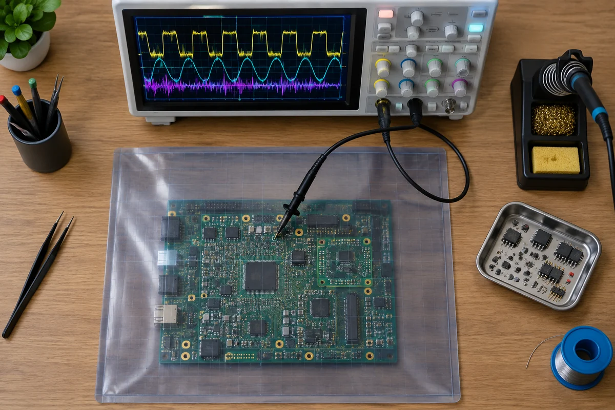
Stress testing approaches for NVMe IP in FPGA environments
SNIA identifies queue configuration, outstanding I/O handling, queue arbitration, and interrupt coalescing as validation challenges.
According to eenewseurope.com, system designers can perform system-level validation of an SoC design’s Ethernet and TCP/IP network interfaces using real network traffic workloads of communication, datacentre, and storage network protocols.
Four stress vectors follow from the validation challenges outlined by SNIA:
| Challenge area | Stress test focus | Typical failure mode |
|---|---|---|
| Queue configuration | Maximum supported queue depth | Queue creation rejected or mis-sized |
| Outstanding I/O handling | Simultaneous command volume | Command timeout or host controller hang |
| Queue arbitration | Priority inversion scenarios | Unfair scheduling or starvation |
| Interrupt coalescing | High-frequency interrupt bursts | Missed interrupts or CPU overload |
For designs targeting network-attached storage, we recommend prioritizing NVMe-over-TCP stress tests. eenewseurope.com describes system-level validation of Ethernet and TCP/IP network interfaces using real network traffic workloads. This validation step may apply to networked architectures.
Verification IP compatibility across FPGA families
NVMe IP verification across FPGA families confirms portability by testing the same IP block through multiple implementation paths.
Our working rule, an opinion rather than a standard: an IP block that passes the same verification through more than one implementation path, on more than one device, can be considered portable.
FPGA families differ in logic density, memory blocks, transceivers and clocking structures. An NVMe host IP verified on one device may need changes in the PCIe hard IP wrapper, clocking or constraints on another: the LDS catalogue, for example, documents a 256-bit AXI interface at 125 MHz for its Gen3 host on Kintex UltraScale+ and at 250 MHz for its Gen4 host on Artix UltraScale+. The verification process, however, remains consistent. The goal is not identical performance but functional compliance with the same requirements on each family.
| Target device | NVMe host interface (LDS catalogue) | Verification focus (our view) |
|---|---|---|
| AMD Kintex UltraScale+ | PCIe Gen3, AXI, 256-bit at 125 MHz | Gen3 throughput, timing closure |
| AMD Artix UltraScale+ | PCIe Gen4, AXI, 256-bit at 250 MHz | Timing closure at 250 MHz, link training |
| Altera Agilex 7 (R-Tile) | PCIe Gen5, Avalon | Avalon adaptation, Gen5 link training |
| Microchip PolarFire | APB registers | Bus adaptation, resource fit |
We structure verification to isolate family-specific dependencies. A testbench that works on one family should work on another with minimal changes, ideally only pin assignments or timing constraints. If extensive modifications are needed, the IP lacks true portability. In a full custom FPGA development workflow, verification is a distinct phase between integration and timing closure, as described in our guide to FPGA design services.
For cross-family compatibility, start with the most constrained family first.
When to use hardware-accelerated verification for NVMe IP
Hardware-accelerated verification for NVMe IP makes sense when software simulation can’t keep up.
Use it when your design hits timing walls or state-space explosions that slow simulation to a crawl. We recommend hardware-accelerated verification when real-time PCIe protocol behavior matters, especially for error recovery and link training sequences. Small designs or early-stage testing, though, rarely need this step: simulation stays faster and cheaper for basic checks.
We recommend hardware acceleration once RTL is stable and you’re chasing corner-case timing or integrating third-party IP with unpredictable latency. The setup overhead only justifies itself when the design’s scale or speed demands it, not as a default choice. For custom FPGA development, this phase fits into the verification and timing closure stages, where hardware tools validate the final bitstream before delivery.
Watch for these signals to decide:
| Choose hardware acceleration when | Stick with simulation when |
|---|---|
| Your design’s logic density or clock domains push simulation beyond practical runtimes | You’re validating basic compliance or early-stage functionality |
| Real-time PCIe protocol behavior (link training, error recovery) is critical to your test plan | The design is small enough that simulation finishes overnight |
| Third-party IP introduces unpredictable latency or timing dependencies | You’re still iterating on RTL and need fast turnaround |
| You’re in the final verification phase before bitstream delivery | Your test cases focus on functional correctness, not timing closure |
NVMe IP verification for data center vs. embedded storage
NVMe IP verification differs for data center and embedded storage by focusing on throughput scalability versus deterministic latency and power constraints.
In data center environments, verification prioritizes high throughput and multi-host scalability. SR-IOV provides hardware-based isolation by subdividing one PCIe interface across multiple virtual machines; Micron describes it for automotive NVMe SSDs, as Electronic Design reports, and the same mechanism serves virtualized data center workloads. A single physical NVMe controller can then serve several virtual machines with hardware isolation.
Embedded storage, by contrast, demands deterministic latency and minimal power consumption. University of Manchester researchers implemented FastPath, an FPGA-based path that accelerates NVMe drive access on a Zynq SoC, and reported up to 71% lower latency than the baseline (FastPath: Towards Wire-Speed NVMe SSDs). Lower latency matters for real-time embedded systems such as automotive ECUs or industrial controllers; worst-case behavior still has to be verified on the target.
Verification strategies reflect these priorities. For data center IP, stress tests simulate multi-tenant workloads with varying queue depths and I/O sizes, while embedded verification focuses on worst-case latency under constrained power budgets. For embedded designs, prioritize verification IP that supports low-latency modes and power-gating hooks. Data center deployments, meanwhile, benefit from IP that includes SR-IOV compliance checks and throughput scaling tests across virtual functions.
| Verification Focus | Data Center | Embedded Storage |
|---|---|---|
| Primary Metric | Throughput (GB/s) | Latency (µs) |
| Key Feature | SR-IOV support | FPGA fast path |
| Power Constraint | Moderate | Strict |
| Verification IP Requirement | Multi-host scalability | Deterministic latency |
These differences extend to the verification workflow itself. Data center IP verification often includes long-duration tests to validate thermal throttling and error recovery under sustained loads, while embedded verification emphasizes corner-case testing for power-state transitions. The choice of verification IP should align with the target environment’s operational profile, not just the NVMe protocol specification.
Latest NVMe protocol versions supported by verification IP
NVMe verification IP should track the current protocol versions to stay compatible with modern SSDs and storage architectures.
| Specification | Latest revision | Ratified |
|---|---|---|
| NVMe Base Specification | 2.4 | 31 July 2026 |
| NVMe over PCIe Transport Specification | 1.4 | 31 July 2026 |
NVM Express released the 2.4 set on 4 August 2026, split into eleven documents, with updates to Zoned Namespaces, Key Value, Rotational Media and Endurance Group Management. Verification IP that lags behind these revisions risks missing edge cases in namespace handling. For FPGA-based designs, this translates to longer debug cycles when integrating SSDs built to newer revisions. Our recommendation: prefer verification IP that explicitly lists the revisions it covers, even if your current project targets older hardware.
Frequently asked questions
What protocol does NVMe use?
NVMe runs over PCIe for direct, high-speed communication with solid-state storage. As EEJournal explains, it manages submission and completion queues as circular buffers and offers a uniform register and command set for PCIe-attached solid-state memories.
How do I know if I have NVMe?
Check your system’s storage controllers for “NVMe” or “Non-Volatile Memory Express” entries. A PCIe-attached SSD that uses the NVMe protocol lists it in its specifications.
What is the latest version of NVMe?
The NVM Express Base Specification revision 2.4, ratified on 31 July 2026 and released with the 2.4 specification set on 4 August 2026, according to NVM Express.
In summary
Start by identifying your design’s critical path: data center deployments need scalability tests, while embedded systems require deterministic latency checks. Run PCIe 5.0 verification for simpler designs, but use PCIe 6.0 tools early to catch PAM4-related bottlenecks. For cross-family compatibility, begin with the most constrained FPGA family to isolate dependencies. Prioritize stress testing for queue depth and command sequencing: these reveal hidden bottlenecks before deployment.
How we wrote this article
The sources we consulted are listed at the end of the article, consulted on 1 October 2026. Where we cite none, it is our opinion, and we write it as such.
This article gives buying criteria and our point of view. It does not replace a professional’s advice on a specific situation.
It is published by Logic Design Solutions, which therefore has an interest in the subject.
Sources
- PCIe for SSDs: EEJournal, eejournal.com
- Cadence adds new capabilities to PCIe VIP including PIPE4 suppo…, eenewseurope.com
- Virtual network co-simulation IP for 800G Ethernet …, eenewseurope.com
- The Role of Centralized Storage in the Emerging Interactive Cockpit | Electronic Design, electronicdesign.com
- NVMe Test Plans | InterOperability Laboratory, iol.unh.edu
- NVMe Based PCIe SSD Validation: Challenges and Solutions | SNIA | Experts on Data, snia.org
- FastPath: Towards Wire-speed NVMe SSDs – Research Explorer The University of Manchester, research.manchester.ac.uk
- NVM Express® Base Specification – NVM Express, nvmexpress.org
- NVMe over PCIe Transport Specification – NVM Express, nvmexpress.org
- FPGA Design Services: What an IP-Focused Design House Delivers – Logic Design Solutions | Logic Design Solutions, logic-design-solutions.com