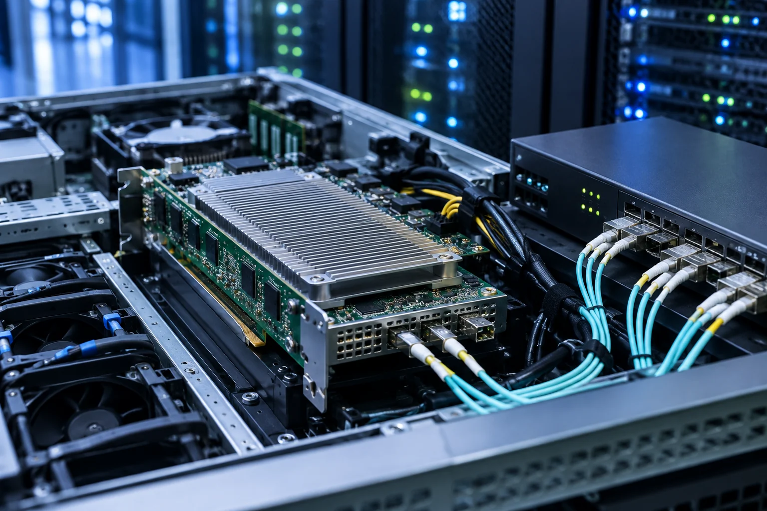
In an FPGA high-frequency trading system, the network boundary separates Ethernet frame handling from application logic. We recommend defining that boundary, and the adjacent storage and host interfaces, before comparing implementation options.
The short answer
For FPGA high-frequency trading, we recommend placing the Ethernet MAC between application logic and PCS/PMA, and specifying its frame-handling role separately from the transceiver path.
Define independent ownership for network, memory, and PCI Express interfaces, including each handoff’s data, producer, consumer, and throughput requirement.
Scope storage IP to an explicit interface contract. Treat BRAM-held order nodes as a limited set of frequently accessed information, not the full database.
Select protocol and FPGA resources from system requirements, and keep software-first open unless those requirements call for custom FPGA logic; published card layouts and latency claims are bounded examples, not whole-system specifications.
Where does FPGA networking fit in a high-frequency trading system?
For an FPGA high-frequency trading design, our recommendation is to define the boundary before comparing implementation options. Draw application logic, the MAC, and PCS/PMA as separate blocks, then state the exact interface in scope. Keep the boundary explicit.
In practical terms, the MAC IP and the accelerator card are described at different levels. Logic Design Solutions describes its 10G Ethernet MAC IP as building and checking IEEE 802.3 frames in FPGA fabric between application logic and a PCS/PMA block. The card announcement, by contrast, describes Ethernet ports on an FPGA-based accelerator card. These descriptions do not provide an end-to-end latency comparison, so do not treat them as interchangeable evidence when choosing a system architecture.
Logic Design Solutions describes its portfolio as a range of FPGA IP cores. For a custom implementation, the company describes an eight-phase engagement, covering specification, architecture and device selection, RTL, integration, timing closure, verification, bring-up, and delivery. Use that sequence to organize the design discussion: start with the requirement, then identify which architecture and interface boundaries need work.
The company also describes its FPGA design services as engineering work that turns a system requirement into a working, verified FPGA design. For an initial architecture review, write down whether the scope is a card, an IP core, or a custom design requirement. Then name the boundary each option needs to address.
Which latency figure describes the Ethernet transceiver path?
Our recommendation for technical notes is to retain the metric, unit, bound, and source together.
How should network, memory and host interfaces be partitioned?
Partition network, memory, and host interfaces by ownership first, then map those logical boundaries to FPGA resources; choose physical placement only after the workload and handoffs are defined.
Treat each boundary as a contract. Name the producer, the block sending data, and the consumer, the block receiving it, along with the exchanged data and required throughput. For the network path, state where frame handling ends and application logic begins; for memory, describe the intended access pattern and storage role; for the host path, define PCI Express responsibilities. Keep ownership explicit. A logical boundary does not automatically require its own FPGA, so keep physical placement a separate decision.
In FPGA partitioning, distinguish the ownership map from the device map: the first assigns interface responsibilities, while the second shows where the logic is placed. That distinction helps keep the design workload-led. Define the logical boundaries before choosing whether to use a multi-FPGA arrangement, rather than letting a board’s layout determine the contracts.
One published card illustrates a possible topology: two Kintex-7 FPGAs connect directly to four SFP+ ports supporting 1 and 10GbE, SONET, and OTN, and each FPGA uses multiple independent banks of QDR-II+ SRAM and DDR3 SDRAM for random access and deep storage, according to the card’s network and memory description. The same card assigns PCI Express to a third FPGA, with sustained bandwidths up to 5 GBytes/sec, as detailed in its PCI Express interface specification.
Use that board as a comparison point, not a template. Its device layout is one implementation; the logical contracts should still reflect the workload and the required handoffs.
Our recommendation is to settle the logical boundaries first, then choose the physical arrangement. Use throughput and interface ownership as explicit design inputs; do not let a published topology make that decision for you.
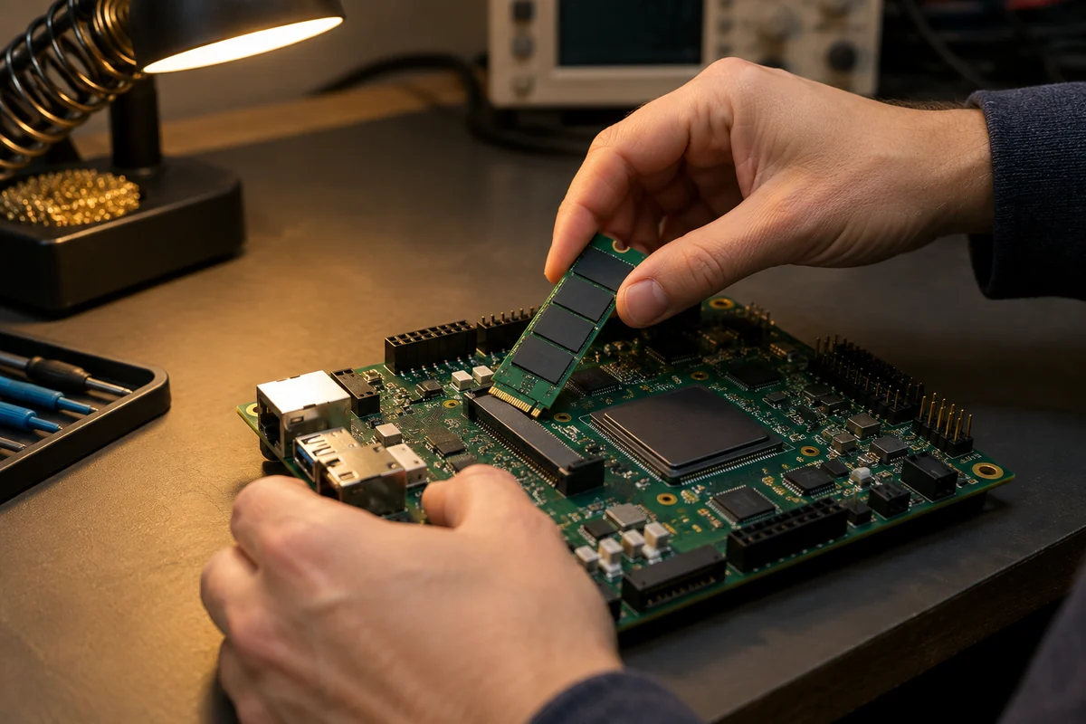
How should engineers scope storage IP against the low-latency network path?
We recommend defining storage IP as a separate requirements contract at its handoff to the low-latency network path, with the allocation tied to the system’s actual requirements.
Start with the boundary. Name the block, the information it receives, and the information it must return. Keep storage responsibilities distinct from network-path responsibilities so an interface requirement does not silently become an assumed storage feature. This is a specification boundary, not a requirement to implement storage as a physically separate block.
Compare a network-interface-only description with a description that also gives storage IP an explicit contract. The latter lets the review focus on which requirements belong to storage and which remain in adjacent logic, without treating the interface as a complete description of storage behavior.
Write down the system requirements that govern the handoff: expected transaction behavior, ordering, error responses, configuration ownership, and reset behavior. Treat these as design inputs rather than details to infer from the network interface. If a requirement does not apply to storage IP, mark it as outside that block’s scope. That keeps the contract bounded instead of turning “storage support” into an open-ended label.
State exactly where each latency target applies. For each target defined by the system, specify whether it belongs to the full request path or to a particular component, then identify the requirements storage IP must meet at the boundary rather than assigning it the network path’s target by implication. The allocation is a system decision, not something the interface should decide silently.
Keep acceptance criteria just as specific. Describe the inputs and outputs to check, the expected responses to valid and invalid transactions, and the conditions for considering the design complete. When the system requirements leave a point open, record it as an unresolved design decision instead of burying it in a broad label.
For a design review, bring a short interface description and a list of requirements owned by the storage block. Use that portfolio context to frame the work, while keeping storage scope tied to the requirements defined for the system.
What role can FPGA-local memory play alongside storage IP?
FPGA-local memory can complement storage IP by holding a compact set of frequently accessed order information, while the order database remains part of the design.
In a trading-system back-end design, the MDPI description of the order-node design says order nodes are stored in BRAM at the same offset as their corresponding orders in the order database. The nodes contain only frequently accessed order information, a choice the paper says optimizes BRAM use.
Our recommendation is to define the BRAM-held node as a deliberately limited representation, not as a copy of every database field. Start by identifying which order information the design needs to access frequently, then keep the node focused on that information and preserve the corresponding offset relationship described in the paper. The key decision is which fields belong in the order node.
Make that decision explicit in the interface and data-structure specification. For each candidate field, ask whether it belongs in the frequently accessed subset that the node is intended to hold. If it does not, leave it out of the node design rather than expanding the structure by default. This keeps the implementation aligned with the cited pattern without assuming that every database field needs a local-memory representation.
Keep the roles distinct in the architecture description: specify the order database, the reduced order node, and how their corresponding offsets relate. Then assess storage IP against the storage requirements it serves, without treating it as interchangeable with the BRAM-held node. The paper supports this specific arrangement; it does not establish a universal field list or prescribe a particular storage-IP configuration.
Keep the boundary clear. A focused node is the design choice.
How should protocol scope influence the network implementation?
Let the system requirement set protocol scope; the forum reply about UDP/IP and TCP/IP describes UDP/IP as simpler and commonly done in FPGAs, but that comparison does not select a protocol for a particular system.
Write down the required protocol first.
Because the cited reply describes UDP/IP as simpler than TCP/IP and commonly done in FPGAs, we treat that as a bounded comparison, not a protocol-selection rule for an individual system. We recommend making the requirement, rather than relative simplicity, the deciding input. Keep the protocol decision explicit in the implementation scope, and separate it from the question of what a particular IP block is expected to do.
| Protocol | What the cited reply says | Scope decision |
|---|---|---|
| UDP/IP | The reply describes UDP/IP as simpler than TCP/IP and commonly done in FPGAs. | Include it when the system requirement calls for it. |
| TCP/IP | The reply names TCP/IP as the comparison for UDP/IP. | Include it when the system requirement calls for it. |
For a useful scope record, state which protocol the system requires, what the FPGA implementation is expected to cover, and which responsibilities are outside that boundary. Keep open questions visible rather than resolving them by assuming that a simpler comparison also means a better fit.
A concrete network-IP boundary is described in the company’s 10G Ethernet MAC IP description: it says the core builds and checks IEEE 802.3 frames in FPGA fabric between application logic and a PCS/PMA block. That gives the scope a specific function and two named endpoints. Record those details when they match the intended block, and state separately which protocol the system requires; the description does not establish that the MAC IP implements UDP/IP or TCP/IP.
Our recommendation is to keep these decisions distinct: choose protocol scope from the system requirement, then describe the selected IP’s stated responsibility and boundaries. Do not infer protocol coverage from the MAC description alone.
Which device resources should engineers compare when selecting an FPGA?
For FPGA high-frequency trading, compare each FPGA device resource named in the design brief under the same workload and implementation assumptions, then rank mandatory needs ahead of preferred headroom.
Start with the design brief.
Our recommendation: build a compact resource-to-requirement matrix and rank feasibility first. For each resource the brief names, record what the design needs it to support, whether that need is mandatory or preferred, and which workload or implementation assumptions shape the comparison. Separate fixed requirements from preferences so optional headroom does not outweigh a constraint the design must meet. This keeps the comparison focused on the intended implementation, rather than on capacity as an abstract score.
When one candidate looks stronger on a single line, keep its ranking provisional until its resource value is compared with the others under the same workload and implementation assumptions, because otherwise the ranking may answer a different design question.
Use the matrix to make three decisions visible:
- Which resource requirements are mandatory?
- Which are preferences rather than constraints?
- What would make a candidate fail the brief?
Keep the record concise: list each candidate’s resource value, the requirement it relates to, and the assumptions behind the comparison. If a requirement is uncertain, mark it as an assumption rather than letting it affect the ranking invisibly. Choose against stated requirements, not an assumed need for maximum capacity. When two candidates meet the mandatory needs, use the remaining preferences to make the trade-off explicit.
When is a software-first implementation a better fit?
For FPGA high-frequency trading, a software-first implementation is the better fit when the requirements define the required behavior without explicitly calling for custom FPGA logic. We recommend that engineers keep the implementation choice open until that boundary is clear.
Programming an FPGA includes developing hardware logic in HDL, such as VHDL or Verilog, to write register transfer logic (RTL), as Electronic Design’s description of FPGA design states. Treat that work as part of the scope decision, not as a label added after requirements are settled.
Start with a requirements record, not a device choice. For each function, record the required behavior, relevant inputs and outputs, and constraints already present in the specification. Put implementation preferences in a separate field. Keep it separate. This gives reviewers a clear distinction between “we would like to use an FPGA” and “the requirement calls for FPGA logic.” Treat high-frequency trading as context for the design question, not as an instruction to select a particular implementation.
Use this comparison to document the decision against stated requirements, rather than assumed advantages:
| Decision path | Use it when | Record |
|---|---|---|
| Software-first | No requirement explicitly calls for custom FPGA logic, and the required behavior can be stated without specifying an FPGA. | The required behavior, stated constraints, and unresolved decisions. |
| FPGA-specific | A stated requirement explicitly calls for custom FPGA logic. | The requirement and the HDL/RTL work included in scope. |
Before changing direction, write down the requirement that would trigger the switch. If none is present, keep software-first as the working choice and leave the FPGA decision open. If one is present, map the requested logic to the scope without extending it beyond what the requirement says.
In summary
We recommend writing an interface scope before choosing an implementation: name the MAC, PCS/PMA, application, storage, memory, and host boundaries, then assign each handoff its owner, exchanged data, throughput needs, and latency target. Mark unowned requirements as open decisions.
Use that scope to compare IP, device resources, or a software-first approach against the same requirements. Keep each performance figure attached to the path and component it describes; do not turn it into a system-wide target.
How we wrote this article
The sources we consulted are listed at the end of the article, consulted on 2 October 2026. Where we cite none, it is our opinion, and we write it as such.
Sector figures come from notre analyse de la base SIRENE de l’INSEE, stock au 1er août 2026. They count establishments; they measure neither output nor sales.
This article gives buying criteria and our point of view. It does not replace a professional’s advice on a specific situation.
It is published by Logic Design Solutions, which therefore has an interest in the subject.
Sources
- First dual Kintex-7 network processor FPGA card …, eenewseurope.com
- comp.arch.fpga | Help me choose an FPGA to design network protocols| page 2, fpgarelated.com
- Reap the Processing Power of FPGA-Integrated SDRs | Electronic Design, electronicdesign.com
- Products – Logic Design Solutions | Logic Design Solutions, logic-design-solutions.com
- 10G Ethernet MAC IP for FPGA: Low-Latency Networking Cores – Logic Design Solutions | Logic Design Solutions, logic-design-solutions.com
- Custom FPGA Development: From Spec to Validated Bitstream – Logic Design Solutions, logic-design-solutions.com
- FPGA Design Services: What an IP-Focused Design House Delivers – Logic Design Solutions, logic-design-solutions.com
- Acceleration of Trading System Back End with FPGAs Using High-Level Synthesis Flow, mdpi.com