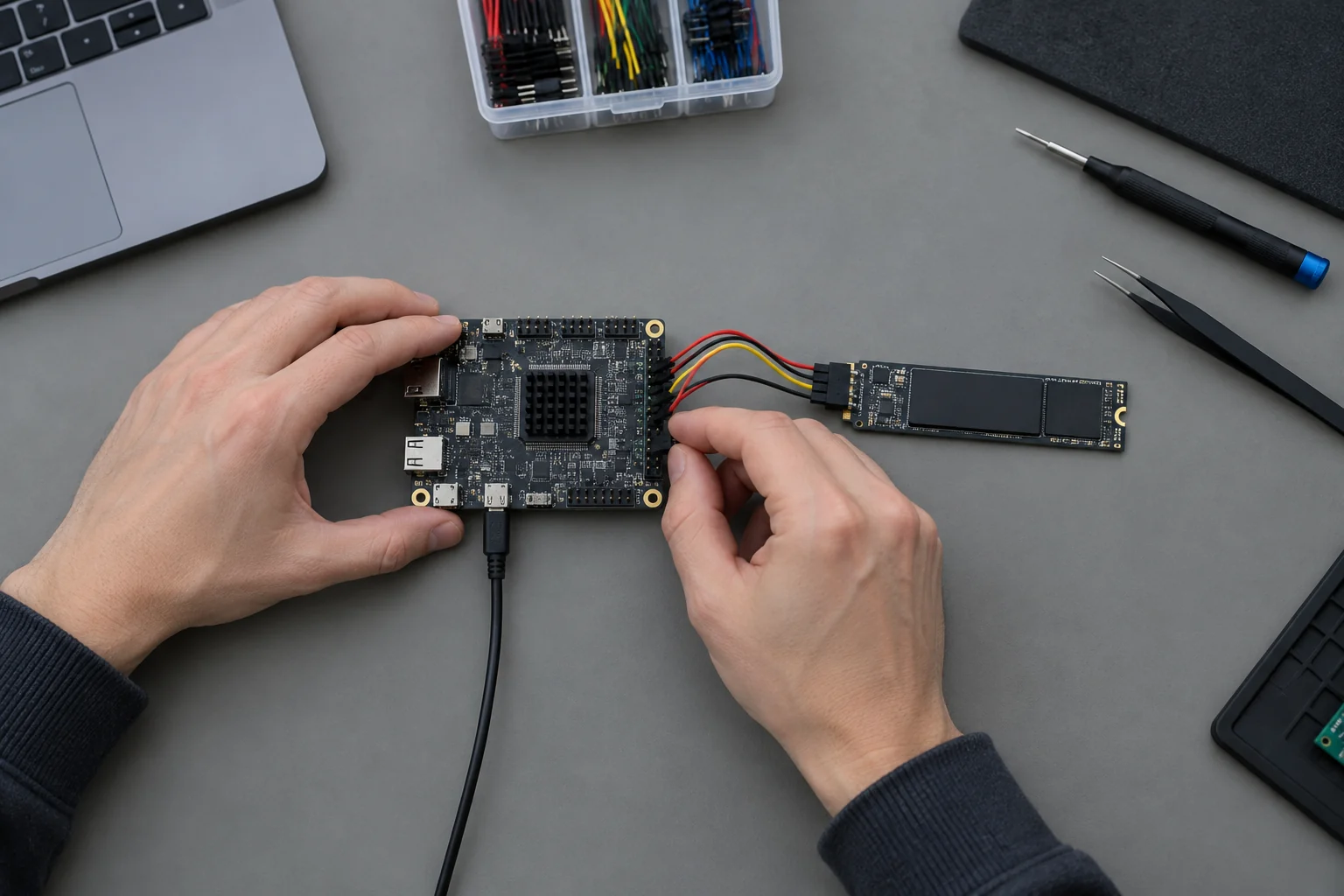
We use “glue logic” narrowly in an FPGA storage design: combinational logic whose outputs depend only on current inputs, with no internal state or memory elements. The key design question is where that boundary ends and protocol progress that must be remembered begins.
The short answer
Glue logic patterns in FPGA storage designs are narrowly scoped combinational decisions: outputs depend only on present inputs, without internal state or memory elements. Use an address decoder, multiplexer, or protocol bridge only when its defined behavior matches that boundary; incompatible protocols call for protocol conversion, while an external interface may use programmable LUT fabric. Keep protocol progress that must be remembered in sequential state registers. When a requirement covers both submission and completion queues in an NVMe queue pair, evaluate protocol-aware storage IP rather than expanding ad hoc glue logic.
What does glue logic mean in an FPGA storage design?
For an FPGA storage design, use “glue logic” for combinational logic connecting functions: its outputs depend only on current inputs, with no internal state or memory elements, as described in this definition of combinational logic.
The same reference lists address decoders, multiplexers, parity generators, ALU datapaths, and priority encoders as examples of combinational logic, and names glue logic between peripherals as another example. Treat these as possible patterns, not a required checklist for a storage design. The pattern depends on the role you are specifying.
We use the output’s dependency as the working boundary. It depends only on current inputs. When documenting a candidate block, write down its present inputs and the output you intend it to produce. For an address decoder or multiplexer, for example, describe the intended input-to-output relationship, then decide whether the description depends only on those present inputs. This keeps the term tied to the behavior under discussion, rather than to a block name alone.
Keep the label precise. When a candidate block’s intended output depends only on its present inputs, describe that behavior as combinational; when the intended behavior includes internal state or memory elements, this definition does not describe that behavior. Name the inputs and intended output in the design notes so the scope of the proposed glue logic stays clear.
If the design uses an IP solution, make the boundary between that solution and the surrounding logic explicit in your design description. Our recommendation: define the glue logic by the behavior you intend to specify, then use that definition consistently when describing the design.
How can glue logic bridge interfaces between IP blocks?
When two IP blocks use incompatible protocols, a converter has to sit between them, the problem addressed by Lee and Park’s paper on protocol converters (Integration, the VLSI Journal, 2002); an FPGA’s flexible, programmable LUT fabric can also bridge external interfaces.
Keep the boundary requirement explicit. Write down the interface each block presents and what the neighboring block expects, then identify whether the issue is protocol incompatibility or a need to bridge an external interface. Protocol compatibility is the deciding condition: when the communicating components use incompatible protocols, consider a converter, as described in the protocol-converter research. For external interfaces, consider the FPGA’s programmable LUT fabric as a bridge, as described in this overview of FPGA interface flexibility.
| Interface situation | Pattern to consider |
|---|---|
| Communicating components use incompatible protocols | Protocol conversion, as described in the protocol-converter research |
| An external interface needs a flexible bridge | Programmable LUT fabric, as described in this FPGA interface overview |
Keep scope narrow. Do not add conversion logic without a defined interface requirement; make the intended boundary behavior clear before choosing the glue logic pattern. For bus conversion, also review how the design handles control signals and payload. A published FPGA bus-conversion design reports that decoupling control signals from payload shortens the extraction FSM’s critical path, according to its design description. Evaluate control and payload separation as a pattern, rather than assuming the reported result applies to every architecture.
Where should combinational glue end and storage-protocol control begin?
Keep combinational glue for decisions based only on inputs at observation, and place protocol progress that must be remembered in sequential state registers, as described by the combinational-circuit definition and MIT’s explanation of state registers.
We recommend drawing the boundary around one question: does the design need to remember protocol progress? If not, keep the decision in combinational glue when it depends only on the input at the time its output is observed. If it must remember progress, put that responsibility in sequential state registers.
| Design question | Combinational glue | Sequential protocol control |
|---|---|---|
| What determines the decision? | The input at the time the output is observed, as described in the combinational-circuit definition. | The current state that the state registers are responsible for remembering, as described in the MIT explanation of state registers. |
| What should the design retain? | Do not assign protocol progress that must be remembered to this category. | Use this category when protocol progress must be remembered. |
Apply the test to each candidate decision rather than to a whole IP boundary. Write down what determines its output, then ask whether the answer depends only on the input present when that output is observed. If so, classify that decision as combinational glue. When the design must remember the current protocol state, assign that responsibility to sequential state registers, whose role is to remember the current state of sequential logic, according to MIT’s state-register explanation.
Which timing paths need review after IP integration?
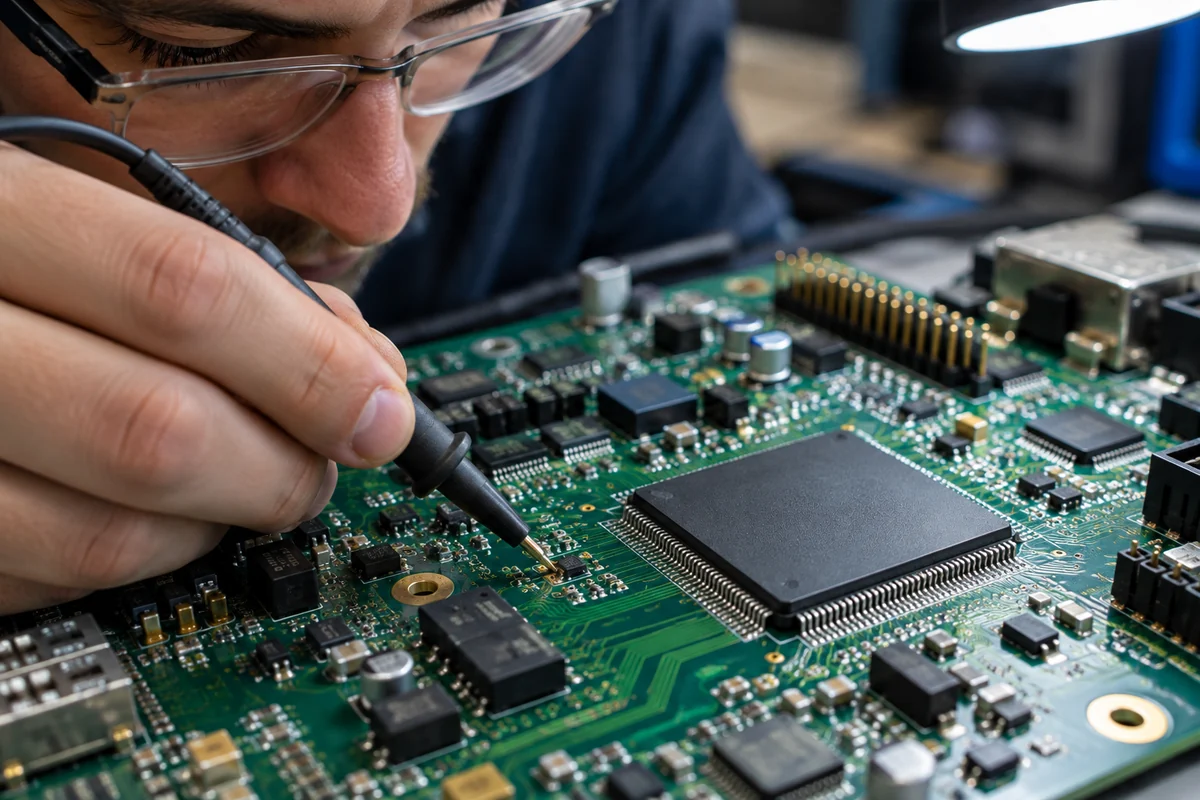
After IP integration, review constrained combinational paths between sequential elements in each clock domain, include short-delay paths alongside long-delay paths, and inspect logic whose inputs may switch at different times, since the output can switch and then return.
We recommend organizing the review by clock domain and recording the paths checked. Start with combinational paths between sequential elements in the same clock domain: the timing-analysis lecture says these paths are constrained and must be analyzed. For each path, note its sequential endpoints and the glue logic included in the review, keeping the record tied to the relevant domain.
Include short-delay paths rather than focusing only on long-delay paths. The FPGA timing lecture warns that a short-delay path could still cause a race condition. In the review record, mark short- and long-delay paths as checked; do not leave the short-delay review implicit.
Also inspect logic whose inputs may switch at different times. SemiEngineering describes an input switching, followed by the other input switching, after which the output switches back. Use an output that changes and then returns as a specific case to consider when reviewing glue logic. Note the input-switching sequence and the related logic in the review record, so the timing-path check and this case are both accounted for.
How does LUT mapping inform resource choices?
LUT mapping informs resource choices by making the objective explicit: prioritize depth with area secondary, prioritize area with depth secondary, or choose duplication-free mapping. The source describes these 3 LUT mapping modes.
| Mapping mode | Objective stated in the source |
|---|---|
| Depth-oriented | Depth is prioritized; area is secondary. |
| Area-oriented | Area is prioritized; depth is secondary. |
| Duplication-free mapping | The description names this mode but does not state an area or depth priority. |
Our recommendation: state the primary objective before choosing a mode. For each glue-logic mapping decision, record whether the choice prioritizes depth, prioritizes area, or uses duplication-free mapping. Keep the two stated priority pairs intact: the source describes depth-oriented mapping with area secondary, and area-oriented mapping with depth secondary.
For duplication-free mapping, record the mode without adding an area-first or depth-first priority that the cited description does not provide.
When should protocol-aware storage IP replace ad hoc glue logic?
Replace ad hoc glue logic when the design boundary must account for both queues in an NVMe queue pair; SPDK defines the pair as 2 queues: a submission queue and a completion queue.
We recommend making queue-pair responsibility the decision point, rather than treating the mere presence of storage as a reason to replace glue logic. Keep a glue-logic pattern narrowly scoped when its stated task does not include both queues; evaluate protocol-aware storage IP first when the requirement includes the queue pair.
| Design requirement | Recommended direction |
|---|---|
| The glue logic has a limited, stated task that does not include both queues. | Keep the pattern limited to that task. |
| The boundary must account for both the submission queue and the completion queue in an NVMe queue pair. | Evaluate protocol-aware storage IP as the first option. |
Before changing the implementation, write a one-line scope statement that names the queue types the boundary is expected to cover, then use that same statement in the RTL design notes and the IP selection criteria. Keep the boundary explicit. If the requirement names both queue types, use the queue pair as the specific scope instead of relying on a broad label such as “storage glue.”
Frequently asked questions
What does “glue logic” mean?
We use “glue logic” for combinational logic connecting functions: its outputs depend only on current inputs, with no internal state or memory elements. Address decoders, multiplexers, parity generators, and priority encoders are possible examples, not a required checklist.
What is glue logic in VLSI design?
In VLSI design, we use the term for combinational logic connecting functional blocks. Its outputs depend only on present inputs, without internal state or memory elements. If protocol progress must be remembered, that responsibility belongs in sequential state registers, not combinational glue.
In summary
Start with one candidate boundary: write down its inputs, intended output, and whether protocol progress must be retained. Classify decisions based only on present inputs as combinational glue; assign remembered progress to sequential state registers. Then record the clock domain and endpoints for timing review, including short-delay paths.
If the requirement names both NVMe queues, evaluate protocol-aware storage IP against that scope. Keep the selection decision open until the specific solution’s queue-pair coverage is explicit.
How we wrote this article
The sources we consulted are listed at the end of the article, consulted on 2 October 2026. Where we cite none, it is our opinion, and we write it as such.
This article gives buying criteria and our point of view. It does not replace a professional’s advice on a specific situation.
It is published by Logic Design Solutions, which therefore has an interest in the subject.
Sources
- Combinational Logic – FPGA Glossary | FPGARelated, fpgarelated.com
- Lattice CrossLinkPlus: EEJournal, eejournal.com
- Glitch Power Issues Grow At Advanced Nodes, semiengineering.com
- Lecture 13: Timing Analysis, eclipse.umbc.edu
- Lecture 15: Physical Design Flow and Timing Analysis, eclipse.umbc.edu
- Heuristics for Area Minimization in LUT-Based FPGA Technology Mapping, eecg.utoronto.ca
- FPGA Design Services: What an IP-Focused Design House Delivers – Logic Design Solutions | Logic Design Solutions, logic-design-solutions.com
- Products – Logic Design Solutions | Logic Design Solutions, logic-design-solutions.com
- Sequential Logic Circuits, bob.cs.sonoma.edu
- 6.1 Annotated Slides | Computation Structures | Electrical Engineering and Computer Science | MIT OpenCourseWare, ocw.mit.edu
- SPDK: Submitting I/O to an NVMe Device, spdk.io